How distributed Bragg reflectors work in LED and VCSEL devices: quarter-wave layer stacks, reflectance and bandwidth design, semiconductor versus dielectric material systems, and the back-side reflector in GaN-based LEDs.
λ/4n (quarter-wave)Layer thickness
> 99%Typical reflectance
Δn up to 1.5Dielectric index contrast
SiO₂ / Ti₃O₅GaN LED stack
Overview
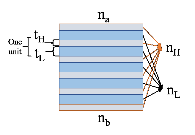
A distributed Bragg reflector (DBR) is a high-efficiency optical reflector built on the principle of Bragg diffraction. It consists of two materials with different refractive indices stacked alternately in a periodic sequence (ABABAB…), as shown in Fig. 1. Each layer is deposited to a precise thickness — normally one quarter of the target wavelength inside that material, λ/4n — so that light at the design wavelength interferes constructively at every interface while other wavelengths cancel out.
Because the phase condition is satisfied at every interface, a well-designed stack reaches very high reflectance — typically above 99% — and can be tuned by adjusting the refractive-index contrast or the layer thicknesses to shift both the centre wavelength and the reflection bandwidth.
Fig. 1Schematic of a distributed Bragg reflector multilayer stack
The Quarter-Wave Condition
The thickness dᵢ of each layer is chosen so that its optical thickness equals one quarter of the reference wavelength λ, following the Bragg reflection relation below. Here nᵢ is the refractive index of that layer, so the physical thickness scales inversely with index: high-index layers are thinner than low-index layers in the same stack.
Eq. 1Quarter-wave thickness condition for each layer in the stack
Reflectance, Bandwidth and Centre Wavelength
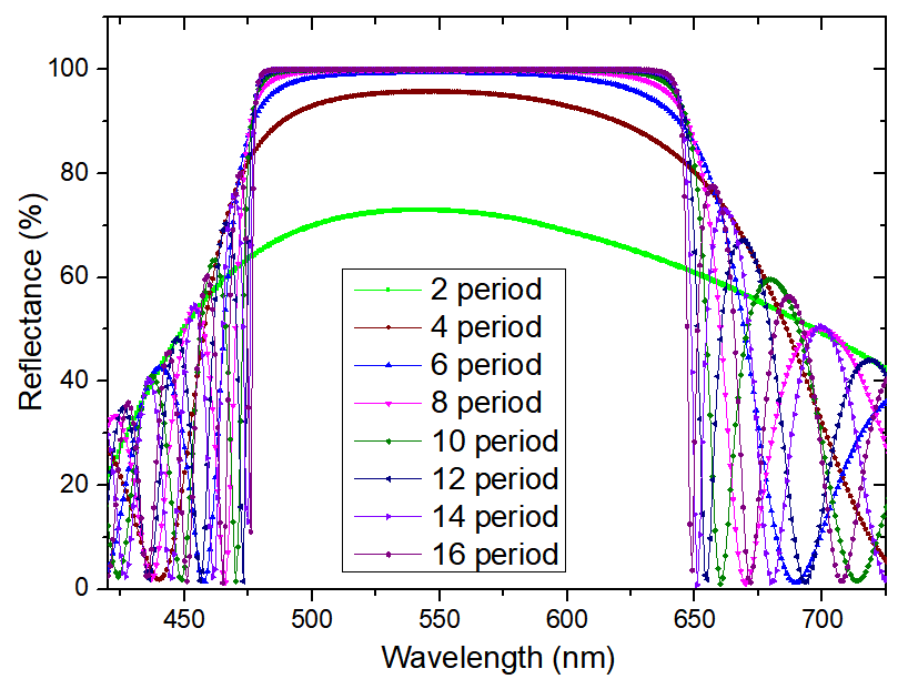
The reflectance of a DBR depends on the refractive-index contrast between the two materials and on the number of periods: the more layers and the more periods, the higher the reflectance, as shown in Fig. 2.
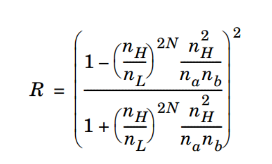
The reflection characteristic is governed by the relations below, where nH and tH are the high-index material and its layer thickness, nL and tL the low-index material and its thickness, λ0 the centre wavelength, Δλ0 the high-reflectance bandwidth, N the number of periods, R the overall reflectance, and na and nb the indices on either side of the stack. Choosing the materials and setting thickness, period count and the remaining parameters lets the stack be designed to a required reflection curve.
Eq. 2Design equations relating layer thickness, period count and reflectanceFig. 2Reflectance as a function of wavelength in a DBR
DBR Material Systems
Two families of materials are used to build DBR stacks: semiconductors and dielectric (insulator) materials.
Semiconductor DBRs
A semiconductor DBR can carry current through the stack, which makes it compatible with vertical current paths. However, lattice-matched semiconductors generally differ only slightly in refractive index, so many layers — and therefore many periods — are needed to reach a high reflectance.
When the stack is built from two semiconductors with different bandgaps, the conduction- and valence-band offsets between them create an electrical barrier that blocks carrier transport — a problem that is especially severe in p-GaN. Doping lowers the resistance, but it simultaneously increases optical absorption in the stack.
Dielectric (Insulator) DBRs
Insulator pairs have a much larger refractive-index difference, so a high reflectance is reached with far fewer pairs. SiO₂/TiO₂ and SiO₂/Ta₂O₅ have become mainstream choices because their index contrast is large — Δn can reach 0.9 to 1.5 — and their deposition processes are mature.
The DBR in a GaN-based LED is typically a SiO₂ / Ti₃O₅ stack, with SiO₂ at a refractive index of 1.46 and Ti₃O₅ at 2.35. SiO₂ is a very important thin-film material because of its low index: it resists decomposition and absorption, scatters well, and is transparent from 160 to 8000 nm, which is why it is so often paired with Ti₃O₅. Ti₃O₅ is widely used in multilayer stacks as well — its refractive index is high, it is transparent in the visible range, and it is very hard.
Semiconductor DBRsSmall index contrast — many periods required
Dielectric (Insulator) DBRsLarge index contrast — few pairs are enough
Fig. 3Layer stack comparison: many thin periods for a semiconductor DBR, versus few thick pairs for a dielectric DBR
Role in GaN-Based LEDs
GaN epitaxial layers are grown on a sapphire substrate, which is highly transparent. After the epi layer electroluminesces, light travelling towards the sapphire side would otherwise be absorbed directly by the packaging material.
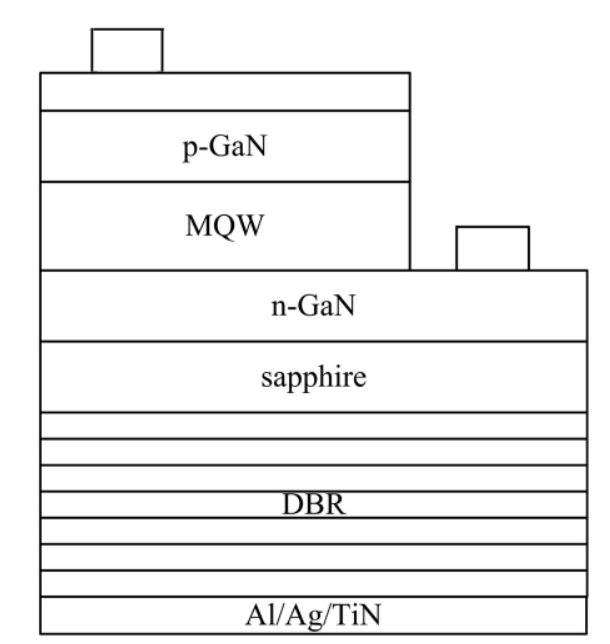
Adding a distributed Bragg reflector — shown in Fig. 4 — reflects that light back out of the device, reducing photon loss and raising the light-extraction efficiency of the LED.
Fig. 4Back-side reflector in an LED chip
GINECHIP Capabilities for DBR and Optical Coatings
GINECHIP deposits optical multilayer stacks in-house and integrates them with the patterning, etch, planarization and bonding steps around them, so a distributed Bragg reflector can be designed, deposited and verified inside one process flow instead of being split across several vendors.
Multilayer stack deposition
PVD sputtering (DC, RF, magnetron, reactive), e-beam and thermal evaporation, PECVD, LPCVD, ALD and electroplating for dielectric and semiconductor multilayer stacks.
Thickness and optical control
Spectroscopic ellipsometry and reflectometry on monitor wafers keep quarter-wave thickness on target across the wafer and from run to run, with periodic process capability reporting.
Materials and substrates
SiO₂, TiO₂, Ta₂O₅, Ti₃O₅, Al₂O₃, HfO₂ and Si₃N₄ films on silicon, sapphire, glass, quartz, GaAs, SiC and GaN-on-sapphire wafers.
Patterning and integration
Photolithography, lift-off, dielectric etch-back, CMP planarization and wafer bonding build the reflector into a complete device flow rather than leaving it as a standalone coating step.
Metrology and quality
SEM, AFM, spectroscopic ellipsometry, optical profilometry, 4-point probe and XRD support every lot, backed by ISO 9001:2015 certification, SEMI standards compliance and ITAR registration.
Volume and flexibility
Single-wafer engineering runs through pilot production on fragments and 100mm to 300mm wafers, with one Certificate of Conformance covering the entire process flow.
Need DBR Thin-Film Stacks on Your Wafers?
GINECHIP deposits dielectric and semiconductor multilayer stacks by sputtering, PECVD, ALD and evaporation, with in-line thickness and optical metrology for LED, VCSEL and photonic device wafers from 100mm to 300mm. Send your target wavelength, reflectance and bandwidth for a process review.