Wafer Reclaim
Chemical-mechanical stripping and repolishing of used test wafers, restored to prime-grade surface quality.
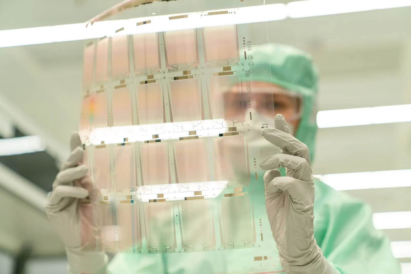
Overview
Wafer reclaim is the process of restoring used, contaminated, or partially processed wafers to virgin-grade quality for reuse as test, monitor, or dummy wafers. For semiconductor fabs, reclaim can reduce wafer procurement costs by 50–70% while supporting sustainability goals. GINECHIP provides ISO-certified reclaim services for silicon, SOI, glass, and compound semiconductor substrates.
Our reclaim process combines selective chemical stripping, precision CMP re-polishing, and comprehensive cleaning and inspection. We handle films including thermal oxide, PECVD oxide/nitride, poly-Si, photoresist, metals (Al, Ti, Cu), and multi-layer stacks. Each reclaimed wafer is re-certified to SEMI standards.
Our Reclaim Services
Film Stripping (Chemical & Dry)
Selective chemical stripping of SiO₂ (HF-based), Si₃N₄ (H₃PO₄ at 160°C), metals (proprietary wet etchants), and photoresist (SPM, EKC, NMP). O₂ plasma ashing for organic residues. Full film removal verified by ellipsometry and XRF. Zero substrate attack guarantee.
CMP Re-Polishing
Chemical-mechanical polishing to restore surface roughness to Ra < 0.5nm (prime-grade). Multi-step polish: bulk removal → fine polish → buff. SiO₂ or CeO₂ slurry systems. In-situ endpoint detection. TTV maintained < 2μm post-reclaim.
Post-Reclaim Cleaning
RCA-1 and RCA-2 clean for organic and metallic contamination removal. Megasonic and brush scrubbing. Final DI water rinse and Marangoni drying. Surface metal contamination < 5×10¹⁰ atoms/cm² (TXRF verified). Particle count < 10 adders @ 0.2μm.
Metrology Re-Certification
Full re-certification package: TTV/bow/warp measurement, surface roughness (AFM), particle count (Surfscan), film residue check (ellipsometry/XRF), and edge inspection. Certificate of Conformance provided. NIST-traceable instrumentation.
Custom Reclaim Development
DOE-based reclaim process development for unique film stacks, exotic substrates (GaAs, SiC, InP, sapphire), and special surface requirements. Process qualification with split-lot testing. Technology transfer support for high-volume production.
Reclaim Process Flow
Incoming Inspection & Sorting
Visual inspection for edge chips and cracks. Film identification via ellipsometry or XRF. Wafer sorting by film type and substrate condition. Lot assignment and traceability.
Chemical Film Stripping
Wet bench processing with heated chemical baths. Recipe-specific chemical sequence. In-line concentration monitoring. DI water cascade rinsing between steps. Exhaust and safety interlocks.
CMP Re-Polishing
Multi-platen CMP: bulk Cu/sacrificial layer removal → fine polish with colloidal silica → final buff. In-situ friction and optical endpoint detection. Post-CMP brush clean and spin-rinse dry.
Post-Reclaim Cleaning
Automated wet bench: RCA-1 (NH₄OH/H₂O₂/DI) → DI rinse → RCA-2 (HCl/H₂O₂/DI) → DI rinse → HF dip (optional) → final rinse → Marangoni dry. Megasonic agitation throughout.
Final Quality Inspection
TTV/bow/warp measurement. Surface roughness (AFM, 5-site sampling). Particle inspection (Surfscan SP1/SP2). Ellipsometry for film residue. Optical microscopy for surface defects. Edge inspection.
Packaging & Certification
Cleanroom-compatible wafer packaging. Certificate of Conformance with full metrology data. Lot traceability and SPC data. Shipment in sealed wafer cassettes or single-wafer shippers.
Reclaim Quality Specifications
| Parameter | Target | Measurement Method |
|---|---|---|
| Surface Roughness (Ra) | < 0.5nm | AFM (10×10μm Scan) |
| TTV (post-reclaim) | < 2.0μm | Capacitive Gauge |
| Bow / Warp | < 30μm (200mm), < 50μm (300mm) | Capacitive Gauge / Interferometry |
| Surface Metal Contamination | < 5×10¹⁰ atoms/cm² | TXRF Analysis |
| Particle Adders (> 0.2μm) | < 10 Adders per Wafer | Surfscan (Laser Light Scattering) |
| Film Residue | Not Detected | Ellipsometry / XRF |
| Edge Exclusion | < 3mm from Wafer Edge | Automated Edge Inspection |
| Reclaim Cycles (before thin-out) | 3–5 Cycles Typical | Thickness Tracking per Cycle |
Specifications above are typical values for the standard reclaim process. Custom reclaim programs are available upon request.
Environmental Benefits
Cost Analysis
Wafer reclaim delivers significant cost savings compared to new prime wafers, typically 60–80% lower cost. For high-volume fabs processing thousands of monitor and test wafers per month, reclaim programs can reduce annual substrate spending by millions of dollars.
Sustainability
Wafer reclaim reduces the environmental footprint of semiconductor manufacturing by extending wafer useful life. Each reclaimed wafer saves approximately 2.5 kWh of energy and 5 liters of water compared to manufacturing a new wafer, while diverting high-purity silicon from waste streams.
Lifecycle Management
Each reclaimed wafer is tracked through its entire lifecycle including reclaim cycle count, remaining thickness, and historical inspection data. Our cycle management system helps you optimize reclaim frequency and predict end-of-life for each wafer.
Substrate Compatibility
Our reclaim processes support silicon wafers of all common dopant types, orientations, and diameters. We also offer reclaim for SOI, glass, and compound semiconductor substrates with dedicated process chemistries for each material system.
Quality Assurance
Our metrology laboratory maintains ISO 17025 accreditation with NIST-traceable reference standards. All measurement equipment undergoes daily calibration verification with certified reference wafers, and our measurement uncertainty is documented for each parameter type.
Start Your Wafer Reclaim Program
Tell us your wafer type, film stack, and monthly volume — we'll design a cost-optimized reclaim process and respond within 24 hours.