Daisy Chain Wafers
Patterned test wafers with daisy-chain interconnect structures for semiconductor package reliability qualification, solder joint integrity testing, and wire bond process validation.
Overview
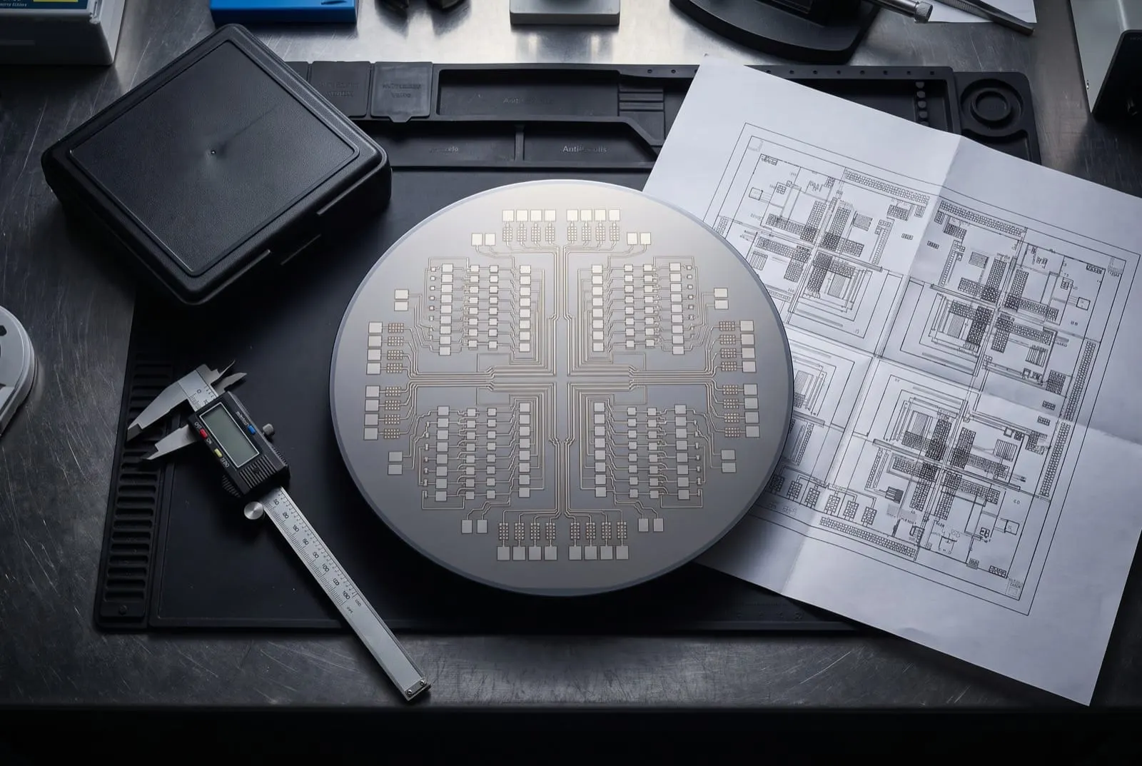
Daisy chain wafers are test vehicles that consist of serially connected metal traces arranged in chains that cross package interconnect boundaries — enabling electrical continuity monitoring across hundreds or thousands of interconnects with a single 2-wire or 4-wire measurement. A single open failure anywhere in the chain is instantly detectable as an open circuit.
Our daisy chain wafers are fabricated on silicon, glass, or SOI substrates with metallization options including Al, Cu, Au, and solder alloys. Designs range from simple single-link chains for wire bond qualification to complex 3D integration test vehicles with thousands of TSV-interconnected links — all fabricated in ISO 9001 certified cleanrooms.
Design Topologies
Our daisy chain wafers support multiple measurement topologies optimized for different failure analysis objectives. Select the configuration that matches your test requirements.
| Parameter | Available Range / Values |
|---|---|
| Chain Type | Single chain, dual chain, interdigitated comb, Kelvin (4-wire), meander |
| Chain Length | 2 to 10,000+ interconnects per chain (custom design) |
| Pad Pitch | 100μm–500μm (standard), 40μm–80μm (fine-pitch probe card) |
| Pad Metallization | Al (AlSi, AlCu), Au, Cu, Ni/Au, ENIG (electroless Ni/immersion Au) |
| Passivation Opening | 50μm × 50μm to 150μm × 150μm (polyimide, PECVD SiO₂/Si₃N₄) |
| Resistance per Link | < 100mΩ (single chain), < 200mΩ (Kelvin chain) |
| Current Handling | Up to 2A per chain (Au/Cu metallization), 500mA (Al metallization) |
Single Daisy Chain
One continuous chain through all interconnects. Simplest layout, fastest test. Detects any open failure but cannot isolate the location. Ideal for pass/fail screening of high-volume packages.
4-Wire Kelvin Chain
Each link has dedicated force and sense connections for precise resistance measurement (±0.1mΩ resolution). Eliminates probe and wiring resistance from the measurement. Essential for detecting subtle degradation from electromigration or corrosion.
Interdigitated Comb Structures
High-sensitivity leakage and insulation resistance test structures. Interdigitated fingers detect surface contamination, ionic migration, and dielectric breakdown between adjacent traces under bias/temperature stress. Suitable for electrochemical migration (ECM) studies per IPC/J-STD standards.
Each daisy chain wafer can include multiple topologies on the same substrate. For example, combine perimeter chains for wire bond testing with area-array Kelvin chains for flip-chip interconnect evaluation on a single reticle field.
Wire Bond Test Vehicles
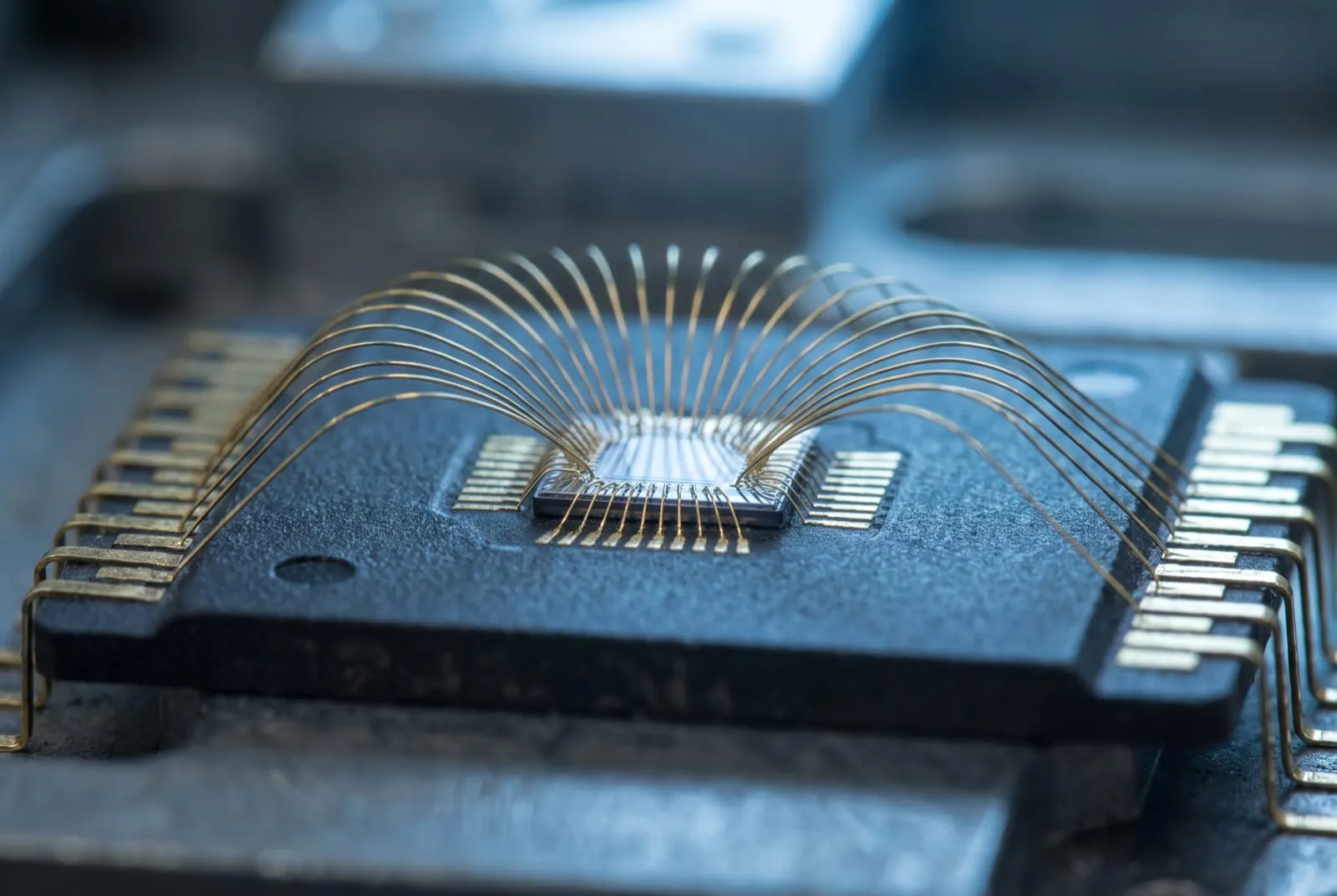
Daisy chain wafers optimized for wire bonding process development and reliability qualification:
| Parameter | Available Range / Values |
|---|---|
| Bond Pad Size | 40μm × 40μm to 150μm × 150μm |
| Bond Pad Metallization | Al (1% Si, 0.5% Cu), Au on TiW barrier, Cu with ENIG finish |
| Pad Thickness | 0.5μm–3.0μm (Al), 0.1μm–1.0μm (Au), 5μm–10μm (ENIG Ni/Au) |
| Wire Type | Au wire (18–50μm), Al wire (18–500μm), Cu wire (18–50μm) |
| Bond Method | Thermosonic ball bonding (Au/Cu), ultrasonic wedge bonding (Al/Au) |
| Test Parameters | Pull test (MIL-STD-883 TM 2011), shear test (TM 2019), cratering test |
Standard Wire Bond Daisy Chain
- Die-to-die, die-to-substrate, or die-to-leadframe chain configurations
- Al, Au, or Cu bond pad metallization with ENIG, ENEPIG, or OSP finish
- Pad pitch: 35–150μm (fine-pitch), 150–500μm (standard)
- Chain lengths: 10–2000+ links per daisy chain
- Optional: integrated heater resistor for in-situ temperature stress
Reliability Stress Testing
- HAST (Highly Accelerated Stress Test): 130°C / 85% RH with continuous or periodic chain resistance monitoring
- Thermal Cycling: -65°C to +150°C, 500–3000 cycles per JEDEC JESD22-A104. In-situ resistance monitoring captures intermittent opens
- High-Temperature Storage (HTS): 150°C–200°C, up to 2000 hours. Monitors intermetallic growth and Kirkendall voiding effects on chain resistance
- Unbiased HAST / Autoclave: High humidity stress without electrical bias. Detects package sealing integrity and moisture ingress paths through chain corrosion
- Custom stress profiles available — contact our engineering team for specialized test requirements
Flip-Chip Test Vehicles
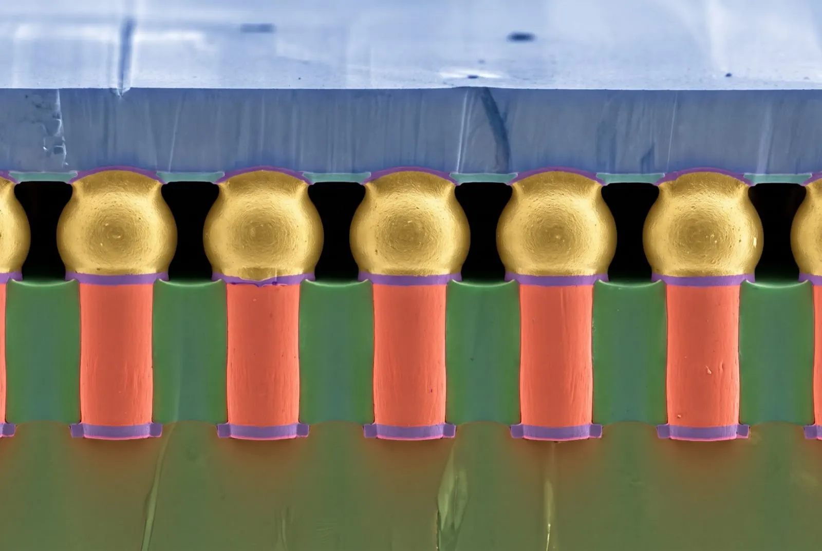
Daisy chain wafers for flip-chip and advanced interconnect qualification:
| Parameter | Available Range / Values |
|---|---|
| Bump Type | Solder bump (SnAg, SAC305, SnPb), Cu pillar + solder cap, Au stud bump |
| Bump Pitch | 150μm–400μm (solder bump), 40μm–130μm (Cu pillar, fine pitch) |
| Bump Height | 50μm–100μm (solder), 10μm–50μm (Cu pillar), 20μm–40μm (Au stud) |
| UBM Stack | Ti/Ni/Au, Ti/Cu/Ni/Au, TiW/Au, Ti/Cu (standard combinations) |
| Daisy Chain Pattern | Perimeter array, full area array, staggered, custom layout |
| Substrate | Si interposer, organic substrate (BT/ABF), glass, ceramic (Al₂O₃, AlN) |
Perimeter Bump Daisy Chain
Standard daisy chain routing through perimeter-array bumps. Daisy chain traces route die edge-to-edge through each bump on two adjacent sides, returning through the opposite sides. Ideal for wire bond replacement and low pin-count flip-chip packages.
- Bump pitch: 100–400μm (perimeter)
- Bump metallurgy: Cu pillar + solder cap, Au stud bump, or solder bump (SAC305, SnAg)
- UBM: Ti/Ni/Au, Ti/Cu, or ENIG with optional OSP
Area-Array (Full Grid) Daisy Chain
2D serpentine routing through full grid-array bumps. Chain visits every bump in the array in a serpentine pattern. Maximizes coverage for comprehensive interconnect reliability assessment.
- Bump pitch: 80–250μm (area array)
- Array sizes: 4×4 to 32×32 and custom
- Detects: non-wet opens, head-in-pillow defects, cracked interconnects, and bump fatigue failures
Cu Pillar Daisy Chain
Optimized for Cu pillar + micro-bump interconnect testing. Fine-pitch capability (down to 40μm pitch). Integrated under-bump metallization (UBM) and solder cap testing.
- Pillar diameter: 15–60μm
- Pillar height: 10–50μm
- Solder cap: SnAg, SAC305, SnBi (low-temp), or AuSn (eutectic)
Through-Silicon Via (TSV) Daisy Chain
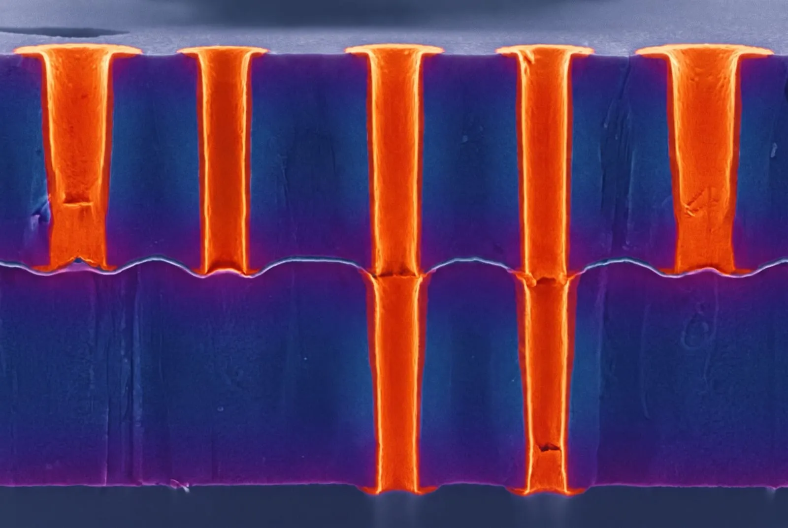
3D integration test vehicles with vertical interconnect chains through the silicon substrate. Daisy chains connect TSVs front-to-back, enabling continuity measurement through the wafer stack.
- TSV diameter: 5–50μm
- TSV depth: 50–300μm (aspect ratio up to 15:1)
- TSV fill: Cu (electroplated), W (CVD), or doped polysilicon
3D Integration Test Vehicles
Advanced test vehicles for 2.5D and 3D heterogeneous integration qualification:
Silicon Interposer Daisy Chain
- Through-interposer via (TIV) chains for continuity testing
- Multi-die daisy chain — tests interposer routing + μbump + C4 bump simultaneously
- RDL daisy chain structures for fan-out wafer-level packaging reliability
- Substrate options: silicon, glass, organic (ABF, Ajinomoto build-up film)
- Compatible with HBM (High Bandwidth Memory) and chiplet integration test protocols
Hybrid Bonding Daisy Chain
- Cu-Cu direct bond interconnect daisy chains with sub-micron alignment accuracy
- Wafer-to-wafer (W2W) and die-to-wafer (D2W) bonding compatibility
- Combined Cu damascene + oxide bonding interface for mechanical and electrical connection
- Contact resistance monitoring per bonded interface pair
- Compatible with post-bond annealing and reliability stress sequences
Custom Test Structure Design
Beyond standard daisy chain topologies, we offer custom test structure design and fabrication for specialized reliability and characterization needs:
Chain Optimization
Variable link resistance chains to detect early degradation, split chains for failure isolation, or addressable matrix chains for pinpoint fault location without physical probing.
Failure Isolation Features
Integrated test pad arrays for 4-wire Kelvin probing at intermediate chain nodes. Embedded heaters and temperature sensors for localized thermal stress application. Designed for easy integration with automated wafer probers.
Custom Metallization Stacks
Multi-layer metallization (up to 6 metal layers) for complex test vehicles. Custom dielectric stacks including SiO₂, SiN, polyimide, and low-k dielectrics. Thick metal options (5–10μm Cu or Au) for high-current interconnect testing.
Applications
Quality & Certification
Our daisy chain wafers are fabricated in ISO 9001 certified cleanroom facilities using established semiconductor manufacturing processes. Each wafer undergoes automated optical inspection (AOI) for pattern integrity, 4-wire Kelvin probing for chain continuity verification (100% electrical test), and dimensional metrology for critical feature verification.
Full documentation package includes: wafer map with pass/fail data per die, GDSII layout file, material and process certificates, chain resistance measurement data, and packaging/handling recommendations. All data is traceable to individual wafer lot numbers.
Need Daisy Chain Wafers for Your Reliability Program?
Tell us your test requirements — chain topology, metallization, substrate, and quantity — and we'll provide a detailed quotation with layout review within 24 hours.