Dummy Die Fabrication
Cost-effective dummy silicon dies for semiconductor packaging R&D, assembly process qualification, thermal simulation, and mechanical stress testing.
Overview
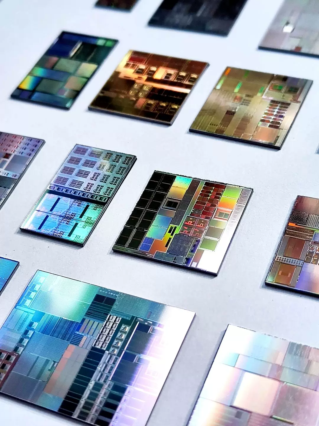
Dummy (or mechanical) dies are non-functional silicon or glass chips that replicate the physical dimensions, weight, and mechanical properties of functional ICs. They are essential for package development, assembly process qualification, wire bonding calibration, and reliability testing — allowing engineers to verify processes without risking expensive functional devices.
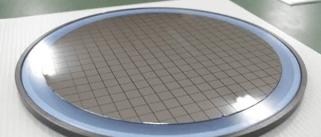
GINECHIP fabricates dummy dies from silicon, glass, ceramic, and metal-coated substrates with precise dimensional control (±5μm tolerance). Available as singulated dies, wafer-form, or custom geometries with optional surface metallization for wire bonding or flip-chip assembly studies.
Product Range
Bare Silicon Dummy Dies
Non-patterned, low-grade silicon wafers or dies for general mechanical testing, process development, and handling trials.
Oxide-Coated Dummy Dies
Thermal oxide (100nm–2μm SiO₂) coated wafers or dies. Used for adhesion studies, surface energy characterization, and dielectric breakdown testing.
Custom-Size Dummy Dies
Dies fabricated to your exact X/Y dimensions and thickness specifications. Ideal for replicating specific IC package outlines for thermal simulation and assembly tooling qualification.
Metallized Dummy Dies
Dies with Al, Au, or Cu pad metallization for wire bonding or flip-chip process development. Pad layout from your GDSII file or standard patterns.
Glass & Ceramic Dummy Dies
Non-silicon dummy substrates. Glass dies for optical package development and transparent assembly observation. Ceramic dies (Al₂O₃, AlN) for high-temperature processes.
Special-Shape Dies & Coupons
Custom geometries including notched dies, T-shaped coupons, multi-thickness wafers, and fragment pieces for specific test fixtures. Drawing-based fabrication with ±25μm tolerance.
Common Applications
Optimize ultrasonic power, bond force, time, and temperature parameters on non-critical dies before processing expensive functional devices.
Validate underfill flow, reflow profiles, and co-planarity requirements using metallized dummy dies before committing to functional flip-chip devices.
Evaluate thermal paste, grease, or phase-change material performance under controlled conditions using standardized dummy die dimensions.
Use dummy dies in board-level reliability testing, 3-point bend tests, and drop/shock testing without consuming functional inventory.
Qualify new pick-and-place equipment, die attach processes, and train operators using low-cost dummy dies before transitioning to production.
Use dummy die assemblies with known intentional defects to calibrate and validate X-ray, CSAM, and other NDT inspection systems.
Cost-Benefit Analysis
Direct Cost Comparison
Dummy dies typically cost 60–80% less than functional prime-grade dies of equivalent dimensions. For a packaging R&D team consuming 500+ dies per month during process development, the annual savings can exceed $50,000–$200,000 depending on die complexity and material.
Total Cost of Ownership
Beyond die cost, dummy dies eliminate the hidden costs of consuming functional inventory: lost revenue from scrapped devices, re-qualification overhead when inventory runs out, and schedule delays from waiting for replacement functional wafers.
Fabrication Design Support
Submit your die dimensions (X, Y, Z), material choice, surface finish requirements, and any special features. Our team reviews your request and provides a DFM assessment with a detailed quotation within 24 hours. We accept DXF, DWG, GDSII, and step files for custom geometries.
Quality Assurance
All dummy dies undergo dimensional inspection (optical metrology, ±5μm tolerance), visual inspection (surface defects, edge chipping), surface roughness verification (if specified), and cleanliness certification (particle count per IEST-STD-CC1246). Full lot traceability maintained from raw material to final shipment.
Need Dummy Dies for Your Packaging Development?
Tell us your die dimensions, material, surface finish, and quantity — we'll provide a competitive quote with delivery timeline within 24 hours.