RDL Bump Wafer
Redistribution layer (RDL) and under-bump metallization (UBM) wafer-level services for advanced packaging.
Overview
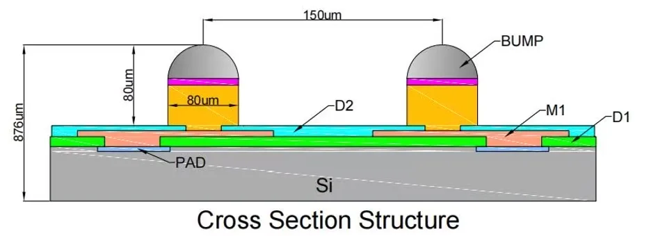
RDL bump wafers are a core technology in advanced packaging, enabling high-density interconnects through redistribution layers (RDL) and under-bump metallization (UBM). GINECHIP offers a full range of RDL and bumping services — including fine-line RDL, copper pillar bumps, solder bumps, and micro-bump technology — supporting 2.5D/3D package integration.
We deliver industry-leading quality and precision, with every RDL and bumping process performed in an ISO Class 5 cleanroom.
RDL Technology Tiers
Standard RDL
Entry-level redistribution layer for cost-sensitive fan-out and flip-chip packages, balancing routing density with high fab yield and fast cycle time.
Fine-Pitch RDL
Multi-layer fine-line RDL using BCB or advanced polyimide dielectrics for denser routing in 2.5D interposers and high-I/O fan-out packages.
Advanced Damascene RDL
Sub-micron damascene copper RDL with CVD SiO₂ dielectric and TaN/Ta barrier, built for the highest interconnect density in 2.5D/3D and chiplet integration.
Bumping Technology Options
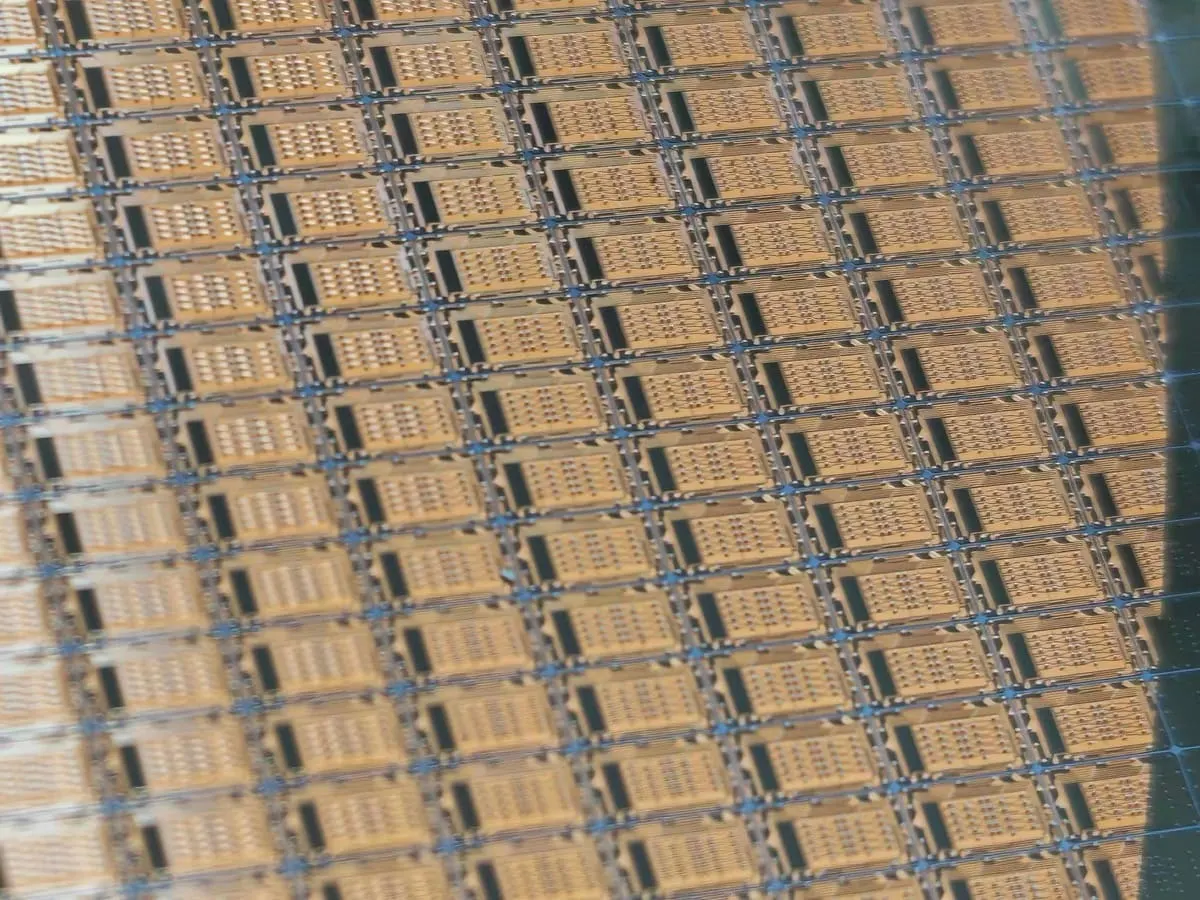
Wafer bumping creates interconnect structures on semiconductor wafers for flip-chip assembly. Our comprehensive bumping platform supports multiple materials, pitches, and aspect ratios across 100mm to 300mm wafers.
Solder Bump
Wafer-level solder bumping in SAC305, SAC405, or SnPb alloys with Ti/Cu or TiW/Cu UBM, ideal for standard flip-chip BGA assembly.
Copper Pillar Bump
High-aspect-ratio copper pillars with SnAg solder caps for finer pitch and lower electrical resistance than conventional solder bumps.
Micro Bump
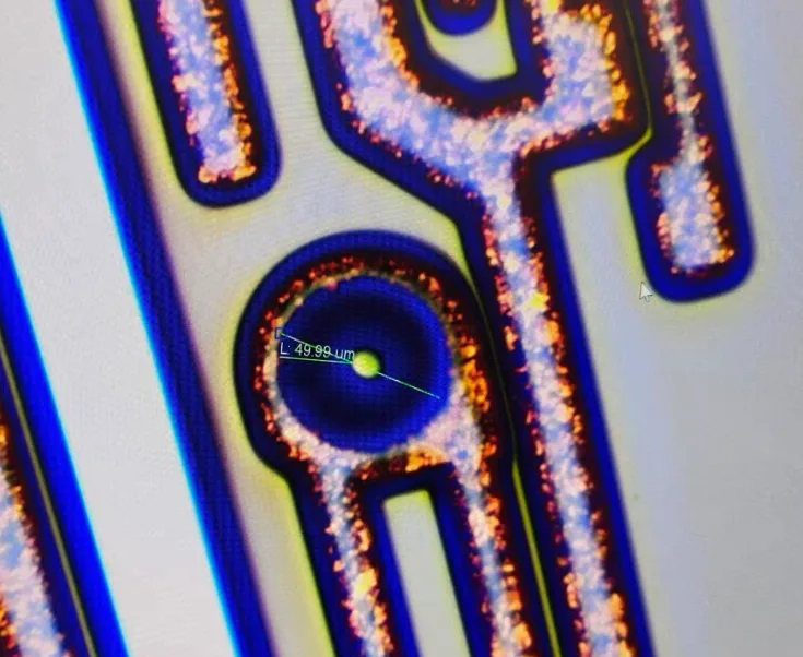
Sub-55μm pitch Cu/Ni/SnAg micro bumps for 2.5D/3D stacking, hybrid bonding, and the tightest interconnect requirements in HBM and chiplet designs.
Bonding Process Flow
Wafer Cleaning & Prep
Incoming wafers undergo particle and organic contaminant removal to establish a clean surface for dielectric coating.
Dielectric Coating & Cure
Polyimide or BCB dielectric is spin-coated and thermally cured to form the insulating base layer for RDL routing.
RDL Photolithography
Photoresist patterning defines the RDL trace geometry, exposed and developed to the target line/space design rule.
Cu Seed Sputtering
A thin copper seed layer is sputter-deposited across the wafer to enable subsequent electroplating.
Cu Electroplating
Copper is electroplated into the patterned traces and vias to build the conductive RDL routing.
UBM Deposition
Under-bump metallization is deposited to provide adhesion, diffusion barrier, and solderable surfaces at each bump site.
Bump Plating & Placement
Solder, copper pillar, or micro bump structures are plated or placed at each UBM site per the selected bump technology.
Reflow & Final Inspection
Bumps are reflowed to final shape, then verified by AOI, cross-section sampling, and electrical continuity testing before release.
Key Applications
RDL and bump layers form the backbone of FOWLP, enabling thinner, smaller packages without a substrate.
Fine-pitch RDL and micro bumps connect interposers and stacked die for high-bandwidth, low-latency system integration.
Solder and copper pillar bumps provide the direct chip-to-substrate connections used in standard flip-chip ball grid array packages.
High-density RDL routing and micro bump interconnects support the massive I/O counts required by AI and HPC compute dies.
Low-loss RDL routing and precision bump placement meet the electrical performance demands of 5G front-end and RF modules.
Compact fan-out and fine-pitch bump solutions deliver the thin-profile, high-I/O packaging mobile application processors require.
Integrated Passive Devices
Integrated Passive Devices fabricated in the RDL layers provide capacitors, inductors, and resistors directly on the wafer surface. IPD integration reduces component count, minimizes parasitics, and improves electrical performance for RF and power management applications.
Quality Assurance & Metrology
Our quality management system is certified to ISO 9001:2015 with additional compliance to SEMI standards, RoHS, REACH, and Conflict Minerals regulations. Each shipment includes a certificate of conformance with lot traceability back to the original ingot.
Ready to Get Started?
Contact our engineering team to discuss your specific requirements and receive a detailed quotation within 24 hours.