프라임 실리콘 웨이퍼
장치 등급 프라임 실리콘 웨이퍼 - 반도체 제조를 위한 최고 품질 등급입니다. CZ 및 FZ 성장 방법, 나노미터 이하의 표면 거칠기, 엄격한 저항률 및 두께 공차. CMOS, MEMS, 전력 장치 및 고급 패키징 라인을 위한 직경 100mm~300mm.
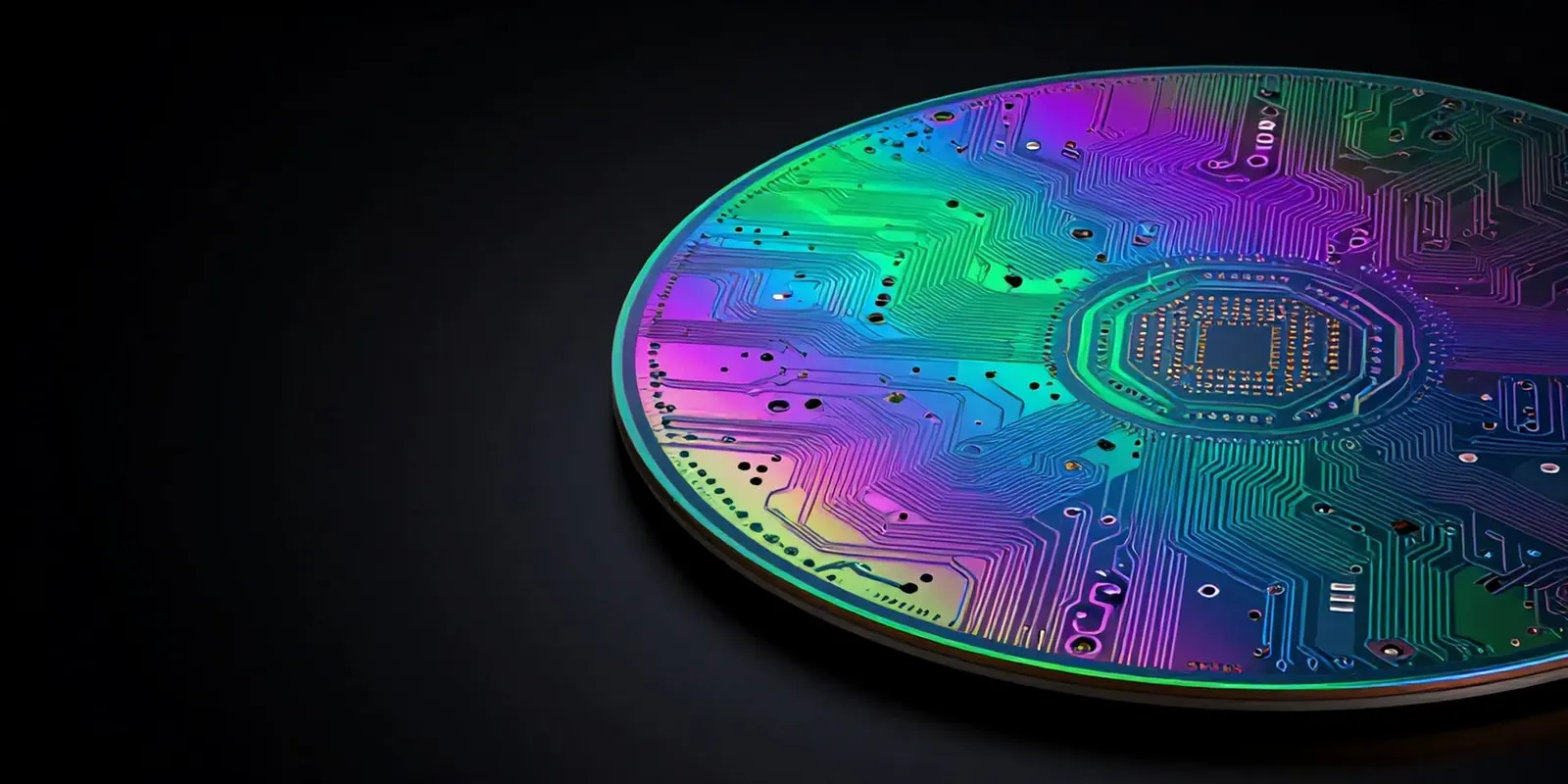
장치 등급 프라임 실리콘 웨이퍼
프라임 등급 실리콘 웨이퍼는 SEMI M1–M13 표준 체계에서 단결정 실리콘 기판의 최고 품질 등급을 나타냅니다. 각 프라임 웨이퍼는 초고순도 폴리실리콘 원료(9N–11N 순도)로 생산되며, 반도체 소자 제조가 요구하는 엄격한 청정도, 평탄도 및 결정학적 완전성을 충족하기 위해 엄격한 결정 성장, 웨이퍼링, 화학기계적 연마 및 세정 공정을 거칩니다.
글로벌 프라임 실리콘 웨이퍼 시장은 연간 출하액 120억 달러를 넘어섰으며, 데이터 센터, 스마트폰, 자동차 전동화 및 IoT 엣지 기기 전반에서 로직, 메모리, 전력 및 아날로그 IC에 대한 끊임없는 수요가 이를 견인하고 있습니다. 첨단 CMOS 노드(sub-5nm)에서 단일 프라임 웨이퍼는 0.2μm에서 파티클 수 10개 미만, 표면 거칠기 0.2nm RMS 미만을 유지해야 하며, 이는 제조 공급망의 모든 단계에 대한 탁월한 제어를 요구하는 사양입니다.
GINECHIP에서는 CZ, MCZ, FZ 방법으로 성장시킨 장치 등급 프라임 웨이퍼를 100mm에서 300mm까지 모든 표준 직경으로 공급합니다. 모든 로트에는 SEMI 및 ASTM 표준에 따라 비저항, 두께, TTV, 보우, 워프, 표면 거칠기, 파티클 수, 산소/탄소 함량을 문서화한 완전한 분석성적서(CoA)가 포함됩니다. COP 프리 아르곤 어닐링 옵션, 후면 폴리실리콘 게터링, 맞춤형 오프컷 방향은 요청 시 제공됩니다.
결정 성장 방법
세 가지 서로 다른 단결정 성장 기술이 프라임 실리콘 웨이퍼를 생산하며, 각각 다른 소자 성능 요구 사항에 최적화되어 있습니다. 올바른 성장 방법을 선택하는 것은 기판 사양에서 가장 영향력이 큰 단일 결정입니다.
CZ (Czochralski)
Melt-growth from a crucible — industry standard
The workhorse of the semiconductor industry. A single-crystal seed is dipped into molten silicon and slowly pulled upward while rotating, producing ingots up to 300mm diameter and 2m+ length. High throughput, moderate oxygen content (12–18 ppma), and excellent cost efficiency for CMOS, logic, memory, and MEMS applications.
MCZ (Magnetic CZ)
Magnetic-field-stabilized Czochralski growth
CZ growth with a strong horizontal magnetic field applied to the melt. The Lorentz force suppresses thermal convection, reducing oxygen incorporation by 30–50% and dramatically improving resistivity radial uniformity. Preferred for power semiconductors (IGBTs, MOSFETs) where precise oxygen control governs lifetime-killer behavior and for high-resistivity substrates used in RFICs.
FZ (Float Zone)
Crucible-free zone-refining — ultimate purity
A molten zone passes along a polycrystalline rod under RF induction in vacuum or inert gas, refining the silicon to extreme purity levels. No crucible contact means carbon and oxygen are below IR detection limits (< 0.1 ppma). Achieves the highest resistivity (up to 10,000+ Ω·cm) and longest minority carrier lifetimes (> 1,000 μs). Essential for high-voltage discrete power devices, photodiodes, RF substrates, and terahertz optics.
등급 비교: CZ vs MCZ vs FZ
CZ, MCZ 및 FZ 기판 중 선택은 목표 소자의 산소 함량, 비저항 범위, 결함 밀도 및 비용 민감도에 대한 요구 사항에 따라 달라집니다. 아래 표는 주요 차별화 요소를 요약한 것입니다.
CZ(초크랄스키)
석영 도가니에서의 표준 용융 성장. 적당한 산소 함량(12–18 ppma)은 금속 오염물의 유익한 내부 게터링을 제공합니다. 최대 300mm의 모든 직경에서 경제적입니다.
MCZ(마그네틱 CZ)
자기장은 용융 대류를 억제하여 산소를 30–50% 줄이고 반경 방향 비저항 균일도를 향상시킵니다. 산소 수준 제어가 필요한 전력 반도체에 최적입니다.
FZ(플로트 존)
도가니가 없는 성장으로 불순물 수준이 IR 검출 한계 미만입니다. 최고 비저항(> 10 kΩ·cm), 최장 캐리어 수명(> 1,000 μs), 최저 산소 함량(< 0.1 ppma).
COP 프리 및 어닐링 프라임 웨이퍼
결정 기원 파티클(COPs)은 CZ 결정 성장 중에 형성되는 나노미터 규모의 공공 응집체로, 직경이 30nm에서 200nm에 이릅니다. 이러한 공공이 연마된 웨이퍼 표면과 교차하면 레이저 검사에서 실제 표면 파티클과 구별할 수 없는 광산란 이벤트로 나타나 잘못된 결함 계수를 초래하고, 첨단 CMOS 공정에서 게이트 산화막 무결성(GOI) 수율을 저하시킵니다.
이를 해결하기 위해 GINECHIP은 SEMI M78에 따라 아르곤 어닐링 프라임 웨이퍼를 제공합니다. 아르곤 또는 수소 분위기에서의 고온 어닐링(≥ 1,200°C)은 표면 근처 영역(일반적으로 3~10μm 깊이)의 COP를 용해하여 COP가 없는 데뉴드 영역을 형성하는 동시에, 웨이퍼 더 깊은 곳의 벌크 산소 석출물을 내부 게터링용으로 보존합니다. 이 처리는 sub-28nm 기술 노드에서 게이트 산화막 두께 3nm 미만이 필요한 소자층에 필수적입니다.
기술 사양
| 매개변수 | 사용 가능 범위/값 |
|---|---|
| Growth Method | CZ (Czochralski), FZ (Float Zone), MCZ (Magnetic CZ) |
| Diameter | 100mm (4″), 125mm (5″), 150mm (6″), 200mm (8″), 300mm (12″) |
| Dopant Type | N-type (Phosphorus, Arsenic, Antimony) / P-type (Boron) |
| Resistivity Range | 0.001 – 10,000 Ω·cm (application-dependent) |
| Crystal Orientation | 〈100〉, 〈111〉, 〈110〉 (off-cut ±0.5° to ±4° on request) |
| Oxygen Content | 12 – 18 ppma (ASTM F121-80), tailored for internal gettering |
| Carbon Content | ≤ 0.1 ppma (ASTM F1319), ultra-low for power devices |
| Thickness Range | 200μm – 1,000μm+ (SEMI M1–M13 standard thicknesses) |
| Thickness Tolerance | ±5μm (200mm), ±10μm (300mm), ±15μm (smaller diameters) |
| TTV (Total Thickness Variation) | ≤ 2μm (200mm), ≤ 3μm (300mm, GBIR per SEMI M1) |
| Bow / Warp | ≤ 20μm Bow, ≤ 25μm Warp (200mm); ≤ 30μm Bow, ≤ 40μm Warp (300mm) |
| Surface Roughness (AFM RMS) | < 0.2nm (1×1μm scan) — Epi-Ready finish |
| Polish Type | SSP (Single-Side Polished) / DSP (Double-Side Polished) |
| Edge Profile | SEMI standard: Round, T-Edge, or E-Edge per diameter |
| Particles @ 0.2μm | ≤ 10 particles (SEMI M53, laser surface scan) |
| COP-Free Option | Argon or Hydrogen annealed — near-zero COPs in near-surface region |
| Backside Treatment | Etched, polished, or poly-silicon back-seal for gettering |
| Laser Mark | SEMI M12/M13 compliant: soft-mark on front or back side |
| Flat / Notch | Per SEMI M1: primary/secondary flats or single notch (200mm/300mm) |
| Warp Control | Edge-Grip or conventional polishing for ultra-flat requirements |
| Packaging | Class 100 cleanroom vacuum-sealed cassette or single-wafer shippers |
| Compliance | SEMI M1–M13, SEMI M53, RoHS, REACH |
응용 및 시장 세그먼트
CMOS Logic & Memory
The backbone of the USD 550B semiconductor industry. Prime CZ wafers serve as starting substrates for microprocessors, DRAM, NAND flash, and SoCs at nodes from 180nm to sub-3nm. Tight particle and surface specifications ensure photolithography yield at advanced nodes.
MEMS & Sensors
Micro-electromechanical systems rely on precisely specified CZ wafers for inertial sensors (accelerometers, gyroscopes), pressure sensors, microphones, and micro-mirrors. DSP wafers with controlled TTV are critical for DRIE etch-through processes and wafer-bonding compatibility.
Power Devices
IGBTs, super-junction MOSFETs, SiC-on-Si epitaxy, and high-voltage diodes demand FZ wafers with resistivity exceeding 1,000 Ω·cm and ultra-low oxygen. MCZ substrates provide the controlled oxygen environment required for optimal lifetime engineering in high-speed power switches.
CMOS Image Sensors (CIS)
Prime wafers with epitaxial silicon layers on heavily-doped substrates provide the gettering capacity and low dark-current characteristics essential for smartphone, automotive, and industrial image sensors. Epi-ready surface quality with sub-0.2nm RMS roughness ensures defect-free epitaxial growth.
Analog / Mixed-Signal
Precision analog ICs — operational amplifiers, ADCs, DACs, voltage references — require wafers with tight resistivity tolerance and minimal dopant striations. FZ substrates with exceptional radial uniformity are preferred for high-performance analog where matching is critical.
Silicon Photonics & Optics
FZ high-resistivity silicon provides the low-loss, low-dispersion optical medium for silicon photonic integrated circuits operating from 1.1μm to 6μm. CZ wafers are used for wafer-level optics, diffractive elements, and structured surfaces in consumer and industrial photonics.
계측 및 품질 보증
모든 프라임 웨이퍼 로트는 ISO 9001:2015 인증 시설에서 다중 기법 계측 프로토콜을 통해 특성화됩니다. 측정된 모든 파라미터를 문서화한 포괄적인 분석성적서(CoA)가 각 출하 시 제공됩니다.
귀하의 팹에 프라임 웨이퍼가 필요하십니까?
직경, 성장 방법(CZ/MCZ/FZ), 도펀트 유형, 비저항 범위, 방향 및 수량을 지정해 주십시오. 당사 기판 전문가가 24시간 이내에 계측 데이터와 리드 타임을 포함한 상세 견적을 제공해 드립니다.