プライムシリコンウェーハ
デバイスグレードのプライムシリコンウェーハ — 半導体製造のための最高品質分類。CZおよびFZ成長法、サブナノメートル表面粗さ、厳格な抵抗率および厚さ公差。100mm~300mm径、CMOS、MEMS、パワーデバイス、先端パッケージング向け。
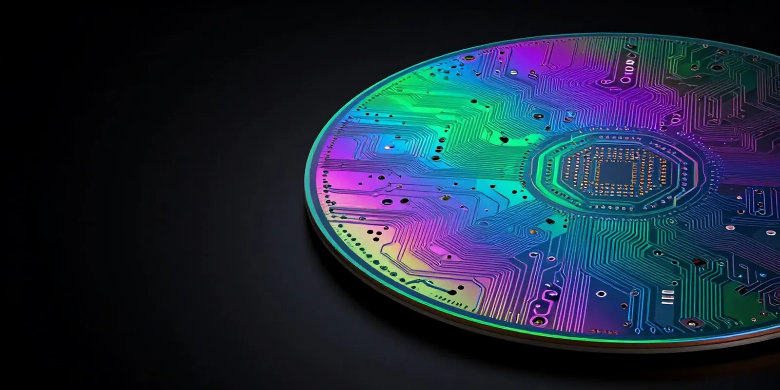
デバイスグレードプライムシリコンウェーハ
プライムグレードシリコンウェーハは、SEMI M1–M13 規格体系における単結晶シリコン基板の最高品質分類です。各プライムウェーハは超高純度ポリシリコン原料(9N–11N純度)から製造され、厳格な結晶成長、ウェーハ化、化学機械研磨、洗浄工程を経て、半導体デバイス製造が要求する厳しい清浄度、平坦度、結晶学的完全性を満たします。
世界のプライムシリコンウェーハ市場は年間出荷額120億米ドルを超え、データセンター、スマートフォン、自動車の電動化、IoTエッジデバイスにおけるロジック、メモリ、パワー、アナログICへの旺盛な需要に牽引されています。先端CMOSノード(sub-5nm)では、1枚のプライムウェーハが0.2μmで粒子数10個未満、表面粗さ0.2nm RMS未満を維持する必要があり、製造サプライチェーンのあらゆる工程に卓越した制御が求められます。
GINECHIPでは、CZ、MCZ、FZ法で成長させたデバイスグレードのプライムウェーハを、100mmから300mmまでのすべての標準直径で供給しています。各ロットには、SEMIおよびASTM規格に準拠した抵抗率、厚さ、TTV、ボウ、ワープ、表面粗さ、粒子数、酸素/炭素含有量を記載した完全な分析証明書(CoA)が付属します。COPフリーのアルゴンアニール、裏面ポリシリコンゲッタリング、カスタムオフカット方位はご要望に応じて対応可能です。
結晶成長方法
3つの異なる単結晶成長技術がプライムシリコンウェーハを製造し、それぞれ異なるデバイス性能要件に最適化されています。正しい成長方法の選択は、基板仕様における最も影響の大きい判断です。
CZ (Czochralski)
Melt-growth from a crucible — industry standard
The workhorse of the semiconductor industry. A single-crystal seed is dipped into molten silicon and slowly pulled upward while rotating, producing ingots up to 300mm diameter and 2m+ length. High throughput, moderate oxygen content (12–18 ppma), and excellent cost efficiency for CMOS, logic, memory, and MEMS applications.
MCZ (Magnetic CZ)
Magnetic-field-stabilized Czochralski growth
CZ growth with a strong horizontal magnetic field applied to the melt. The Lorentz force suppresses thermal convection, reducing oxygen incorporation by 30–50% and dramatically improving resistivity radial uniformity. Preferred for power semiconductors (IGBTs, MOSFETs) where precise oxygen control governs lifetime-killer behavior and for high-resistivity substrates used in RFICs.
FZ (Float Zone)
Crucible-free zone-refining — ultimate purity
A molten zone passes along a polycrystalline rod under RF induction in vacuum or inert gas, refining the silicon to extreme purity levels. No crucible contact means carbon and oxygen are below IR detection limits (< 0.1 ppma). Achieves the highest resistivity (up to 10,000+ Ω·cm) and longest minority carrier lifetimes (> 1,000 μs). Essential for high-voltage discrete power devices, photodiodes, RF substrates, and terahertz optics.
グレード比較:CZ vs MCZ vs FZ
CZ、MCZ、FZ基板の選択は、目標デバイスの酸素含有量、抵抗率範囲、欠陥密度、コスト感度に対する要件によって決まります。以下の表は主要な差別化要因をまとめたものです。
CZ(チョクラルスキー法)
石英坩堝内での標準的な融液成長。適度な酸素含有量(12–18 ppma)が金属汚染物質の有益な内部ゲッタリングを提供します。300mmまでのすべての直径で経済的です。
MCZ(磁場印加CZ法)
磁場が融液対流を抑制し、酸素を30–50%低減して半径方向の抵抗率均一性を向上させます。酸素レベルを制御する必要があるパワー半導体に最適です。
FZ(フローティングゾーン法)
坩堝を使わない成長で、不純物レベルは赤外検出限界未満。最高の抵抗率(> 10 kΩ·cm)、最長のキャリア寿命(> 1,000 μs)、最低の酸素含有量(< 0.1 ppma)。
COPフリー・アニールプライムウェーハ
結晶起因パーティクル(COP)は、CZ結晶成長中に形成されるナノメートルスケールの空孔集合体であり、直径は30nmから200nmに及びます。これらの空孔が研磨ウェーハ表面と交差すると、レーザー検査において真の表面パーティクルと区別できない光散乱事象として現れ、誤った欠陥カウントを引き起こし、先端CMOSプロセスにおけるゲート酸化膜品質(GOI)歩留まりを低下させます。
これに対応するため、GINECHIPはSEMI M78に準拠したアルゴンアニールプライムウェーハを提供します。アルゴンまたは水素雰囲気中での高温アニール(≥ 1,200°C)は、表面近傍領域(通常3–10μm深さ)のCOPを溶解し、COPフリーのデヌードゾーンを形成すると同時に、ウェーハ深部のバルク酸素析出物を内部ゲッタリング用に保持します。この処理は、sub-28nm技術ノードでゲート酸化膜厚3nm未満を必要とするデバイス層に不可欠です。
技術仕様
| パラメータ | 利用可能範囲/値 |
|---|---|
| Growth Method | CZ (Czochralski), FZ (Float Zone), MCZ (Magnetic CZ) |
| Diameter | 100mm (4″), 125mm (5″), 150mm (6″), 200mm (8″), 300mm (12″) |
| Dopant Type | N-type (Phosphorus, Arsenic, Antimony) / P-type (Boron) |
| Resistivity Range | 0.001 – 10,000 Ω·cm (application-dependent) |
| Crystal Orientation | 〈100〉, 〈111〉, 〈110〉 (off-cut ±0.5° to ±4° on request) |
| Oxygen Content | 12 – 18 ppma (ASTM F121-80), tailored for internal gettering |
| Carbon Content | ≤ 0.1 ppma (ASTM F1319), ultra-low for power devices |
| Thickness Range | 200μm – 1,000μm+ (SEMI M1–M13 standard thicknesses) |
| Thickness Tolerance | ±5μm (200mm), ±10μm (300mm), ±15μm (smaller diameters) |
| TTV (Total Thickness Variation) | ≤ 2μm (200mm), ≤ 3μm (300mm, GBIR per SEMI M1) |
| Bow / Warp | ≤ 20μm Bow, ≤ 25μm Warp (200mm); ≤ 30μm Bow, ≤ 40μm Warp (300mm) |
| Surface Roughness (AFM RMS) | < 0.2nm (1×1μm scan) — Epi-Ready finish |
| Polish Type | SSP (Single-Side Polished) / DSP (Double-Side Polished) |
| Edge Profile | SEMI standard: Round, T-Edge, or E-Edge per diameter |
| Particles @ 0.2μm | ≤ 10 particles (SEMI M53, laser surface scan) |
| COP-Free Option | Argon or Hydrogen annealed — near-zero COPs in near-surface region |
| Backside Treatment | Etched, polished, or poly-silicon back-seal for gettering |
| Laser Mark | SEMI M12/M13 compliant: soft-mark on front or back side |
| Flat / Notch | Per SEMI M1: primary/secondary flats or single notch (200mm/300mm) |
| Warp Control | Edge-Grip or conventional polishing for ultra-flat requirements |
| Packaging | Class 100 cleanroom vacuum-sealed cassette or single-wafer shippers |
| Compliance | SEMI M1–M13, SEMI M53, RoHS, REACH |
アプリケーションと市場セグメント
CMOS Logic & Memory
The backbone of the USD 550B semiconductor industry. Prime CZ wafers serve as starting substrates for microprocessors, DRAM, NAND flash, and SoCs at nodes from 180nm to sub-3nm. Tight particle and surface specifications ensure photolithography yield at advanced nodes.
MEMS & Sensors
Micro-electromechanical systems rely on precisely specified CZ wafers for inertial sensors (accelerometers, gyroscopes), pressure sensors, microphones, and micro-mirrors. DSP wafers with controlled TTV are critical for DRIE etch-through processes and wafer-bonding compatibility.
Power Devices
IGBTs, super-junction MOSFETs, SiC-on-Si epitaxy, and high-voltage diodes demand FZ wafers with resistivity exceeding 1,000 Ω·cm and ultra-low oxygen. MCZ substrates provide the controlled oxygen environment required for optimal lifetime engineering in high-speed power switches.
CMOS Image Sensors (CIS)
Prime wafers with epitaxial silicon layers on heavily-doped substrates provide the gettering capacity and low dark-current characteristics essential for smartphone, automotive, and industrial image sensors. Epi-ready surface quality with sub-0.2nm RMS roughness ensures defect-free epitaxial growth.
Analog / Mixed-Signal
Precision analog ICs — operational amplifiers, ADCs, DACs, voltage references — require wafers with tight resistivity tolerance and minimal dopant striations. FZ substrates with exceptional radial uniformity are preferred for high-performance analog where matching is critical.
Silicon Photonics & Optics
FZ high-resistivity silicon provides the low-loss, low-dispersion optical medium for silicon photonic integrated circuits operating from 1.1μm to 6μm. CZ wafers are used for wafer-level optics, diffractive elements, and structured surfaces in consumer and industrial photonics.
計測・品質保証
各プライムウェーハロットは、ISO 9001:2015認証施設において多手法の計測プロトコルでキャラクタリゼーションされます。測定されたすべてのパラメータを記載した包括的な分析証明書(CoA)が各出荷に添付されます。
ファブ向けプライムウェーハが必要ですか?
直径、成長方法(CZ/MCZ/FZ)、ドーパントタイプ、抵抗率範囲、方位、数量をご指定ください — 当社の基板スペシャリストが24時間以内に計測データとリードタイムを含む詳細な見積もりを提供します。