פרוסות סיליקון ראשיות
פרוסות סיליקון ראשיות בדרגת התקן — סיווג האיכות הגבוה ביותר לייצור מוליכים למחצה.
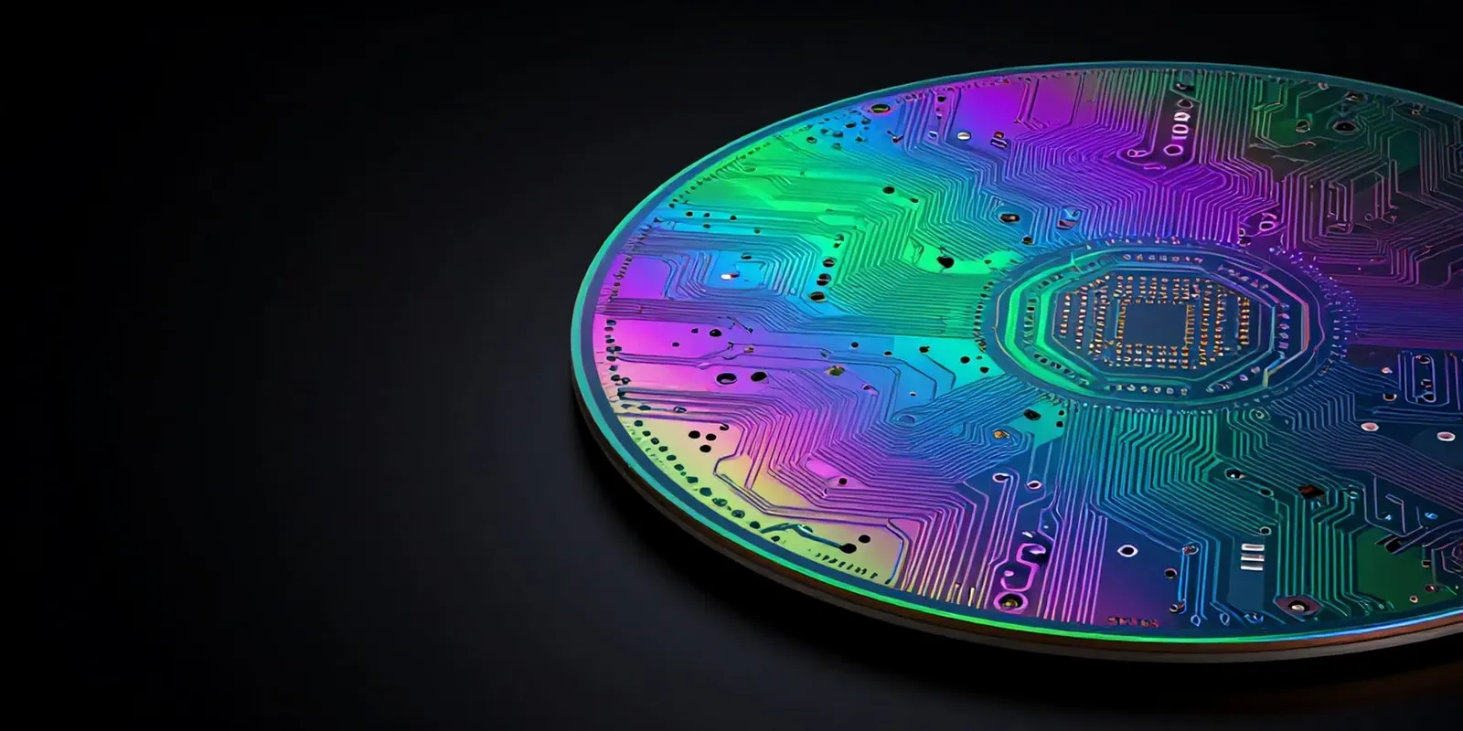
פרוסות סיליקון ראשיות בדרגת התקן
פרוסות סיליקון בדרגת פריים מייצגות את סיווג האיכות הגבוה ביותר של מצעי סיליקון חד-גבישיים בהיררכיית התקנים SEMI M1–M13. כל פרוסת פריים מיוצרת מחומר גלם פוליסיליקון בטוהר על (טוהר 9N–11N) ועוברת תהליכי גידול גביש, חיתוך פרוסות, ליטוש כימי-מכני וניקוי קפדניים, כדי לעמוד בדרישות הניקיון, השטיחות והשלמות הגבישית המחמירות של ייצור התקנים מוליכים למחצה.
שוק פרוסות הסיליקון בדרגת פריים העולמי חצה 12 מיליארד דולר במשלוחים שנתיים, מונע מהביקוש הבלתי פוסק ל-IC לוגיים, זיכרון, הספק ואנלוגיים במרכזי נתונים, סמארטפונים, חשמול רכב והתקני קצה IoT. בצמתי CMOS מתקדמים (sub-5nm), פרוסת פריים בודדת חייבת לשמור על ספירת חלקיקים מתחת ל-10 ב-0.2μm ועל חספוס פני שטח מתחת ל-0.2nm RMS — מפרטים הדורשים שליטה יוצאת דופן בכל שלב בשרשרת האספקה.
ב-GINECHIP אנו מספקים פרוסות פריים בדרגת התקן הגדלות בשיטות CZ, MCZ ו-FZ בכל הקטרים הסטנדרטיים מ-100mm עד 300mm. כל אצווה כוללת תעודת ניתוח מלאה (CoA) המתעדת התנגדות סגולית, עובי, TTV, בואו, ווארפ, חספוס פני שטח, ספירת חלקיקים ותכולת חמצן/פחמן לפי תקני SEMI ו-ASTM. אפשרויות נטולות COP עם אניל בארגון, גטור פוליסיליקון בצד אחורי ואוריינטציות off-cut מותאמות זמינות לפי בקשה.
שיטות גידול גבישים
שלוש טכנולוגיות גידול חד-גבישי נפרדות מייצרות פרוסות סיליקון בדרגת פריים, כל אחת מותאמת לדרישות ביצועים שונות של התקנים. בחירת שיטת הגידול הנכונה היא ההחלטה בעלת ההשפעה הרבה ביותר במפרט המצע.
CZ (Czochralski)
Melt-growth from a crucible — industry standard
The workhorse of the semiconductor industry. A single-crystal seed is dipped into molten silicon and slowly pulled upward while rotating, producing ingots up to 300mm diameter and 2m+ length. High throughput, moderate oxygen content (12–18 ppma), and excellent cost efficiency for CMOS, logic, memory, and MEMS applications.
MCZ (Magnetic CZ)
Magnetic-field-stabilized Czochralski growth
CZ growth with a strong horizontal magnetic field applied to the melt. The Lorentz force suppresses thermal convection, reducing oxygen incorporation by 30–50% and dramatically improving resistivity radial uniformity. Preferred for power semiconductors (IGBTs, MOSFETs) where precise oxygen control governs lifetime-killer behavior and for high-resistivity substrates used in RFICs.
FZ (Float Zone)
Crucible-free zone-refining — ultimate purity
A molten zone passes along a polycrystalline rod under RF induction in vacuum or inert gas, refining the silicon to extreme purity levels. No crucible contact means carbon and oxygen are below IR detection limits (< 0.1 ppma). Achieves the highest resistivity (up to 10,000+ Ω·cm) and longest minority carrier lifetimes (> 1,000 μs). Essential for high-voltage discrete power devices, photodiodes, RF substrates, and terahertz optics.
השוואת דרגות: CZ מול MCZ מול FZ
הבחירה בין מצעי CZ, MCZ ו-FZ תלויה בדרישות התקן היעד לתכולת חמצן, טווח התנגדות סגולית, צפיפות פגמים ורגישות לעלות. הטבלה שלהלן מסכמת את הגורמים המבדילים העיקריים.
CZ (צ׳וכרלסקי)
גידול מתוך נוזל תקני בכור Quartz. תכולת חמצן מתונה (12–18 ppma) מספקת גטור פנימי מועיל של מזהמים מתכתיים. כלכלי בכל הקטרים עד 300mm.
MCZ (CZ מגנטי)
שדה מגנטי מדכא קונבקציית הנוזל, מפחית חמצן ב-30–50% ומשפר אחידות התנגדות רדיאלית. מיטבי למוליכים למחצה הספק הדורשים רמות חמצן מבוקרות.
FZ (אזור צף)
גידול ללא כור עם רמות זיהומים מתחת לגבול גילוי IR. התנגדות סגולית גבוהה ביותר (> 10 kΩ·cm), זמן חיים ממוצע של נושאים ארוך ביותר (> 1,000 μs) ותכולת חמצן נמוכה ביותר (< 0.1 ppma).
פרוסות פריים נטולות COP ואניל
חלקיקים ממקור גבישי (COPs) הם חללים אגרגטיים בקנה מידה ננומטרי הנוצרים במהלך גידול גביש CZ — בקוטר שבין 30nm ל-200nm. כאשר חללים אלה חותכים את משטח הפרוסה המלוטשת, הם מופיעים בבדיקת לייזר כאירועי פיזור אור שאינם ניתנים להבחנה מחלקיקי שטח אמיתיים, וגורמים לספירת פגמים שגויה הפוגעת בתפוקת שלמות תחמוצת השער (GOI) בתהליכי CMOS מתקדמים.
כדי לטפל בכך, GINECHIP מציעה פרוסות פריים עם אניל בארגון לפי SEMI M78. אניל בטמפרטורה גבוהה (≥ 1,200°C) בסביבת ארגון או מימן ממיס COPs באזור הסמוך לפני השטח (בדרך כלל בעומק 3–10μm), ומייצר אזור נקי נטול COP תוך שימור משקעי חמצן נפחיים לגטור פנימי בעומק הפרוסה. טיפול זה חיוני לשכבות התקן הדורשות עובי תחמוצת שער מתחת ל-3nm בצמתי טכנולוגיה sub-28nm.
מפרטים טכניים
| פרמטר | טווח / ערכים זמינים |
|---|---|
| Growth Method | CZ (Czochralski), FZ (Float Zone), MCZ (Magnetic CZ) |
| Diameter | 100mm (4″), 125mm (5″), 150mm (6″), 200mm (8″), 300mm (12″) |
| Dopant Type | N-type (Phosphorus, Arsenic, Antimony) / P-type (Boron) |
| Resistivity Range | 0.001 – 10,000 Ω·cm (application-dependent) |
| Crystal Orientation | 〈100〉, 〈111〉, 〈110〉 (off-cut ±0.5° to ±4° on request) |
| Oxygen Content | 12 – 18 ppma (ASTM F121-80), tailored for internal gettering |
| Carbon Content | ≤ 0.1 ppma (ASTM F1319), ultra-low for power devices |
| Thickness Range | 200μm – 1,000μm+ (SEMI M1–M13 standard thicknesses) |
| Thickness Tolerance | ±5μm (200mm), ±10μm (300mm), ±15μm (smaller diameters) |
| TTV (Total Thickness Variation) | ≤ 2μm (200mm), ≤ 3μm (300mm, GBIR per SEMI M1) |
| Bow / Warp | ≤ 20μm Bow, ≤ 25μm Warp (200mm); ≤ 30μm Bow, ≤ 40μm Warp (300mm) |
| Surface Roughness (AFM RMS) | < 0.2nm (1×1μm scan) — Epi-Ready finish |
| Polish Type | SSP (Single-Side Polished) / DSP (Double-Side Polished) |
| Edge Profile | SEMI standard: Round, T-Edge, or E-Edge per diameter |
| Particles @ 0.2μm | ≤ 10 particles (SEMI M53, laser surface scan) |
| COP-Free Option | Argon or Hydrogen annealed — near-zero COPs in near-surface region |
| Backside Treatment | Etched, polished, or poly-silicon back-seal for gettering |
| Laser Mark | SEMI M12/M13 compliant: soft-mark on front or back side |
| Flat / Notch | Per SEMI M1: primary/secondary flats or single notch (200mm/300mm) |
| Warp Control | Edge-Grip or conventional polishing for ultra-flat requirements |
| Packaging | Class 100 cleanroom vacuum-sealed cassette or single-wafer shippers |
| Compliance | SEMI M1–M13, SEMI M53, RoHS, REACH |
יישומים ופלחי שוק
CMOS Logic & Memory
The backbone of the USD 550B semiconductor industry. Prime CZ wafers serve as starting substrates for microprocessors, DRAM, NAND flash, and SoCs at nodes from 180nm to sub-3nm. Tight particle and surface specifications ensure photolithography yield at advanced nodes.
MEMS & Sensors
Micro-electromechanical systems rely on precisely specified CZ wafers for inertial sensors (accelerometers, gyroscopes), pressure sensors, microphones, and micro-mirrors. DSP wafers with controlled TTV are critical for DRIE etch-through processes and wafer-bonding compatibility.
Power Devices
IGBTs, super-junction MOSFETs, SiC-on-Si epitaxy, and high-voltage diodes demand FZ wafers with resistivity exceeding 1,000 Ω·cm and ultra-low oxygen. MCZ substrates provide the controlled oxygen environment required for optimal lifetime engineering in high-speed power switches.
CMOS Image Sensors (CIS)
Prime wafers with epitaxial silicon layers on heavily-doped substrates provide the gettering capacity and low dark-current characteristics essential for smartphone, automotive, and industrial image sensors. Epi-ready surface quality with sub-0.2nm RMS roughness ensures defect-free epitaxial growth.
Analog / Mixed-Signal
Precision analog ICs — operational amplifiers, ADCs, DACs, voltage references — require wafers with tight resistivity tolerance and minimal dopant striations. FZ substrates with exceptional radial uniformity are preferred for high-performance analog where matching is critical.
Silicon Photonics & Optics
FZ high-resistivity silicon provides the low-loss, low-dispersion optical medium for silicon photonic integrated circuits operating from 1.1μm to 6μm. CZ wafers are used for wafer-level optics, diffractive elements, and structured surfaces in consumer and industrial photonics.
מטרולוגיה והבטחת איכות
כל אצוות פרוסות פריים מאופיינת בפרוטוקול מטרולוגיה רב-טכנולוגי במתקנים בהסמכת ISO 9001:2015. תעודת ניתוח מקיפה (CoA) המתעדת את כל הפרמטרים הנמדדים מסופקת עם כל משלוח.
צריך פרוסות פריים לפאב שלך?
ציינו את הקוטר, שיטת הגידול (CZ/MCZ/FZ), סוג המאלח, טווח ההתנגדות הסגולית, האוריינטציה והכמות — מומחי המצעים שלנו יספקו הצעת מחיר מפורטת עם נתוני מטרולוגיה וזמן אספקה בתוך 24 שעות.