As the semiconductor industry grapples with the slowing pace of Moore’s Law, advanced semiconductor packaging has emerged as a critical pathway to enhance system performance and reduce costs. This in-depth report explores the technologies, market dynamics, and key players shaping the future of chip packaging, moving beyond traditional scaling to achieve greater integration and functionality.
The Role of Packaging in the Semiconductor Value Chain
Packaging is a crucial step in the semiconductor manufacturing process, serving to protect the delicate die, provide electrical connectivity, and dissipate heat. It bridges the gap between the microscopic world of the chip and the macroscopic world of the printed circuit board (PCB). The primary goals of packaging are to protect the chip, support its physical structure, connect its electrodes to external circuits, and enhance thermal performance.
Packaging materials are typically plastic, ceramic, or metal. Plastic is the most common and cost-effective but offers the least thermal dissipation. Ceramic provides better heat management but is more expensive. Metal offers the best thermal performance but requires an insulating layer, so it is often used as a cap on plastic or ceramic packages.
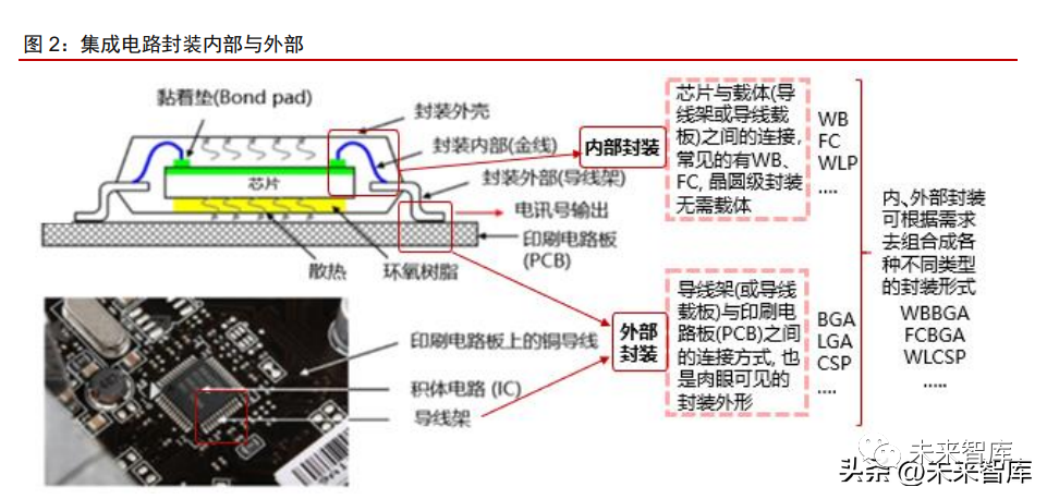
Packaging can be categorized by its connection structure. Internal packaging refers to the connection between the die and its carrier (lead frame or substrate), with common methods including wire bonding (WB) and flip-chip (FC). External packaging is the visible form factor connecting the carrier to the PCB, such as QFP, QFN, and BGA. Wafer-level packaging (WLP) bypasses traditional carriers, connecting the die directly to the PCB.
Why Advanced Packaging? The Post-Moore’s Law Imperative
For decades, the industry relied on shrinking transistor sizes to double performance every 18-24 months, a trend known as Moore’s Law. However, as process nodes become increasingly complex and expensive, the cost and time required for each new generation have skyrocketed. This has led to a paradigm shift where system-level integration, rather than pure transistor scaling, is key to improving performance.
Advanced packaging enables this integration by combining multiple dies, or chiplets, into a single package. This approach offers several advantages:
- Cost Reduction: Manufacturing smaller dies improves yield and lowers cost. These dies can then be integrated into a single package, as seen with AMD’s chiplet architecture.
- Performance Gains: By integrating dies with high-bandwidth interconnects, performance can be significantly boosted. Apple’s M1 Ultra chip, which combines two M1 Max dies using TSMC’s InFO-LSI technology, is a prime example.
- Heterogeneous Integration: Dies manufactured on different process nodes (e.g., logic and memory) can be combined, optimizing performance and cost for each function.
Key Advanced Packaging Technologies
Advanced packaging is broadly divided into substrate-based and wafer-level categories, each with its own set of technologies and applications.
Substrate-Based Packaging
These packages use a substrate or interposer to connect multiple dies.
- FCBGA (Flip-Chip Ball Grid Array): This technology combines flip-chip interconnects with a BGA substrate. It offers excellent electrical performance, high I/O density, and good thermal dissipation, making it ideal for high-performance ASICs, CPUs, and GPUs.
- Embedded SiP (System-in-Package): Dies are embedded directly into the substrate, reducing connection distances and improving power efficiency and thermal performance. This is widely used in power management ICs and sensors.
Wafer-Level Packaging (WLP)
WLP is performed on the wafer before dicing, allowing for a smaller final package.
- Fan-In WLP: The package size is essentially the same as the die size. It is used for applications with a limited number of I/Os, such as power management and RF chips.
- Fan-Out WLP: The package extends beyond the die area, allowing for more I/Os. This is achieved by reconstituting the wafer with a mold compound and creating a redistribution layer (RDL). It is used for high-performance, low-power applications in mobile devices.
2.5D and 3D Integration
These are the most advanced packaging technologies, enabling high-density vertical and horizontal integration.
- 2.5D Integration: Dies are placed side-by-side on a silicon interposer that contains TSVs (Through-Silicon Vias) for high-bandwidth connections. This is used for high-performance computing and network applications.
- 3D Integration: Dies are stacked vertically, connected by TSVs and micro-bumps. This offers the highest density and performance but is also the most complex. TSMC’s SoIC and Intel’s Foveros are leading examples.
Market Outlook and Growth Drivers
The advanced packaging market is poised for significant growth. According to Yole, the global advanced packaging market is expected to grow from $30.4 billion in 2020 to over $50 billion by 2025, a CAGR of over 10%. This growth is driven by several factors:
- Demand from 5G and IoT: The proliferation of 5G devices and IoT applications requires highly integrated, miniaturized packages like SiP for RF modules and sensors.
- High-Performance Computing (HPC): The need for faster and more efficient processors for AI, data centers, and autonomous driving is fueling demand for 2.5D/3D packaging and chiplet-based designs.
- Consumer Electronics: The trend towards thinner, lighter, and more feature-rich mobile devices is driving adoption of wafer-level and fan-out packaging.
The SiP market is expected to reach $18.8 billion by 2025, while the 2.5D/3D market is projected to hit $11.8 billion. Fan-out wafer-level packaging is the fastest-growing segment, with a CAGR of nearly 20%.
Competitive Landscape: Foundries, IDMs, and OSATs
The advanced packaging landscape is becoming increasingly competitive, with players from different parts of the semiconductor value chain vying for market share.
- Foundries (e.g., TSMC, Samsung): These companies are leveraging their advanced wafer manufacturing capabilities to offer leading-edge packaging solutions like CoWoS, InFO, and SoIC. They are particularly strong in 2.5D/3D and fan-out technologies.
- IDMs (e.g., Intel): Intel has developed its own advanced packaging technologies, such as EMIB and Foveros, primarily for its own products.
- OSATs (e.g., ASE, JCET, Amkor): These outsourced assembly and test companies are focusing on SiP and other packaging forms. They hold a strong position in heterogeneous integration and are key players in the SiP market.
While foundries dominate the most advanced 2.5D/3D technologies, OSATs are expected to remain strong in SiP and other areas, benefiting from the broad demand for system-level integration.
China’s Advanced Packaging Industry
China is a major player in the global packaging market, driven by its large domestic demand for semiconductors. The country’s advanced packaging market was valued at over RMB 90 billion in 2020, and it is growing rapidly due to the push for domestic self-sufficiency.
Key Chinese OSATs include:
- JCET (Jiangsu Changjiang Electronics Technology): The largest OSAT in China, offering a wide range of advanced packaging technologies including FC, SiP, and 2.5D/3D.
- Tongfu Microelectronics: Specializes in high-end packaging for CPUs and GPUs, with strong capabilities in flip-chip and chiplet packaging.
- Huatian Technology: A major player with a focus on traditional packaging, expanding into advanced areas like CIS (CMOS Image Sensor) packaging and SiP.
- China WLCSP (Jingfang Technology): A leader in wafer-level packaging for sensors, achieving high margins through its specialized focus.
These companies are investing heavily in advanced packaging capacity and technology, positioning themselves to benefit from the ongoing trend of domestic substitution.
Conclusion
Advanced semiconductor packaging is no longer just a back-end process; it is a strategic technology for extending the benefits of Moore’s Law. As the industry moves towards heterogeneous integration and chiplet-based designs, the role of packaging in determining system performance, cost, and form factor will only grow. With a dynamic competitive landscape and strong market drivers, advanced packaging is set to be a cornerstone of the semiconductor industry for the next decade and beyond.
Source: Original WeChat article