AI chip power consumption is climbing from hundreds of watts toward thousands of watts, but what truly challenges thermal engineers is not total power—it’s uneven heat distribution. GPUs don’t heat uniformly: certain regions run exceptionally hot, HBM stacks generate their own heat, and I/O and power delivery networks add to the thermal load. The more integrated the package, the more heat sources and the more concentrated the hot spots.
The old thermal logic was simple: chip generates heat → package encloses it → heatsink attached on top. Advanced packaging flips this paradigm. The new logic asks: how are chips arranged, where does heat originate, what path does it take, which materials does it pass through, and what cooling method is used—all decided together during the design phase.
In the AI chip era, packaging is no longer just an “interconnect technology.” It’s a systems engineering discipline that determines performance, power, thermal behavior, yield, and reliability. Advanced packaging solves thermal challenges not through a single technique but through thermal path restructuring.
1. Spreading Heat Sources: Chiplet Layout Reduces Hot Spot Overlap
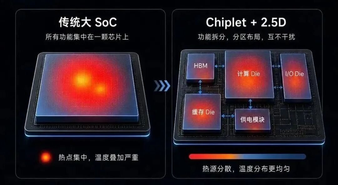
Traditional large SoCs integrate compute cores, cache, I/O, and power delivery into a single die. All functions concentrate in one place, hot spots overlap, and temperatures spike. The Chiplet + 2.5D packaging approach breaks functions apart and distributes them: compute dies, I/O dies, cache dies, and HBM stacks are placed independently, maintaining distance between high-heat sources to prevent overlapping temperature rises and leaving room for heat flow.
This reduces overall thermal risk at the design source—not by stacking multiple furnaces together, but by spreading them out so heat becomes easier to manage.
2. Lateral Heat Spreading: Interposers and Substrates as More Than Wiring Platforms
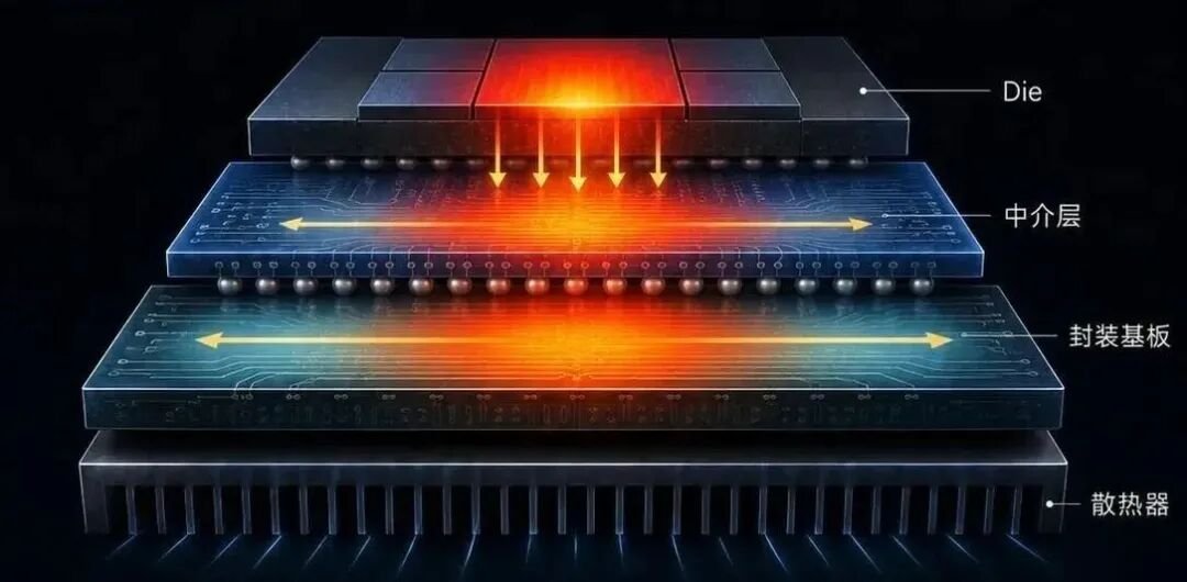
Silicon interposers offer good thermal conductivity but come with high cost and size limitations. RDL/organic substrates provide more flexibility and larger form factors, yet face thermal conductivity and coefficient of thermal expansion (CTE) challenges. The value of interposers and packaging substrates lies in spreading heat laterally from the dies before handing it off to the heatsink.
Package thermal design must balance thermal conductivity, mechanical stress, warpage, and solder joint reliability. Thermal management isn’t just about conducting heat—it’s about making trade-offs among materials, stress, and reliability.
3. Making Heat Flow Easier from Chip to Heatsink: Optimizing TIM
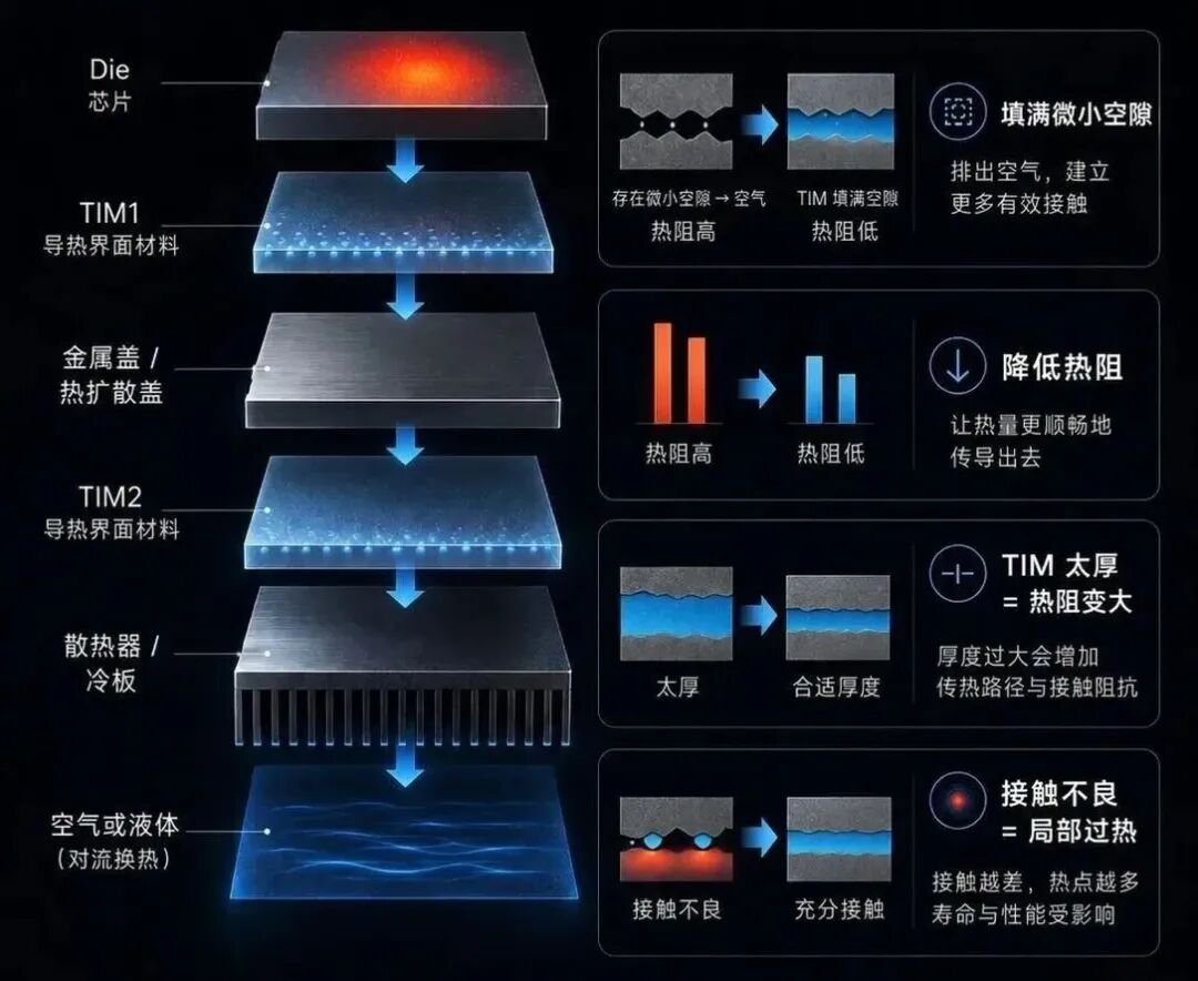
Thermal Interface Materials (TIM) fill the microscopic gaps between the die and the heat spreader, displacing air and establishing effective contact. High thermal resistance means heat gets trapped; low resistance means smooth heat transfer. TIM that’s too thick increases resistance, while TIM that’s too thin creates poor contact and localized hot spots.
TIM acts as “thermal glue”—the thinner, more uniform, and better the contact, the easier heat escapes.
4. Turning Small Hot Spots into Large-Area Heat Sources: Metal Heat Spreaders
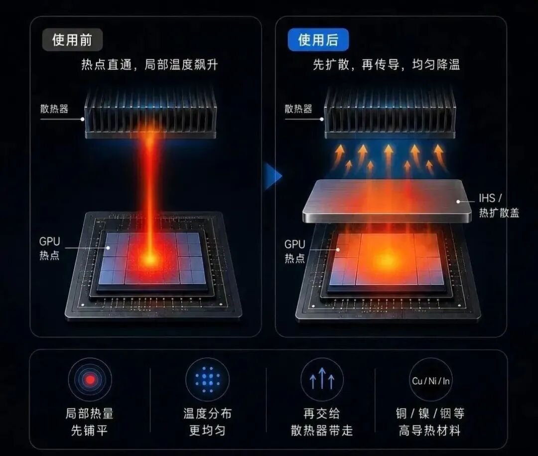
An Integrated Heat Spreader (IHS) doesn’t cool directly. Its value is to “flatten” heat from localized hot spots, spreading it uniformly across a larger area before handing it to the heatsink. Materials like copper, nickel, and indium are used to fabricate IHS—using high-thermal-conductivity materials to equalize temperature first, then dissipate.
5. After Stacking, Heat Must Escape: Vertical Cooling in 3D Packaging
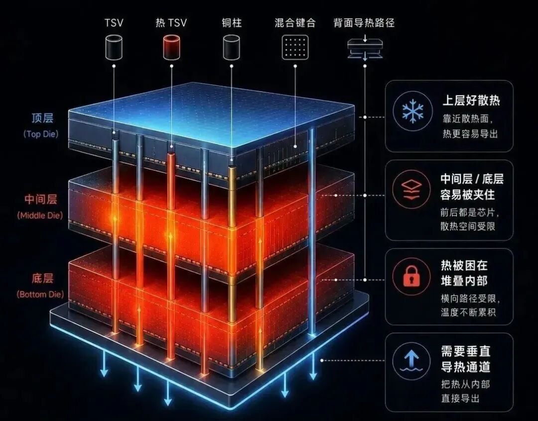
In 3D stacking, the top die sits closest to the cooling surface and dissipates heat most easily. Middle layers get sandwiched with limited cooling access. Bottom dies face constrained lateral paths, causing temperature buildup. Heat trapped inside the stack requires vertical thermal conduits to escape directly from within.
The core of 3D cooling isn’t stacking higher—it’s providing escape routes for heat. Thermal TSVs, copper pillars, hybrid bonding, and backside thermal paths all serve as vertical channels built for heat.
6. Bringing Coolant Closer to the Heat Source: From Air to Liquid to Microchannels
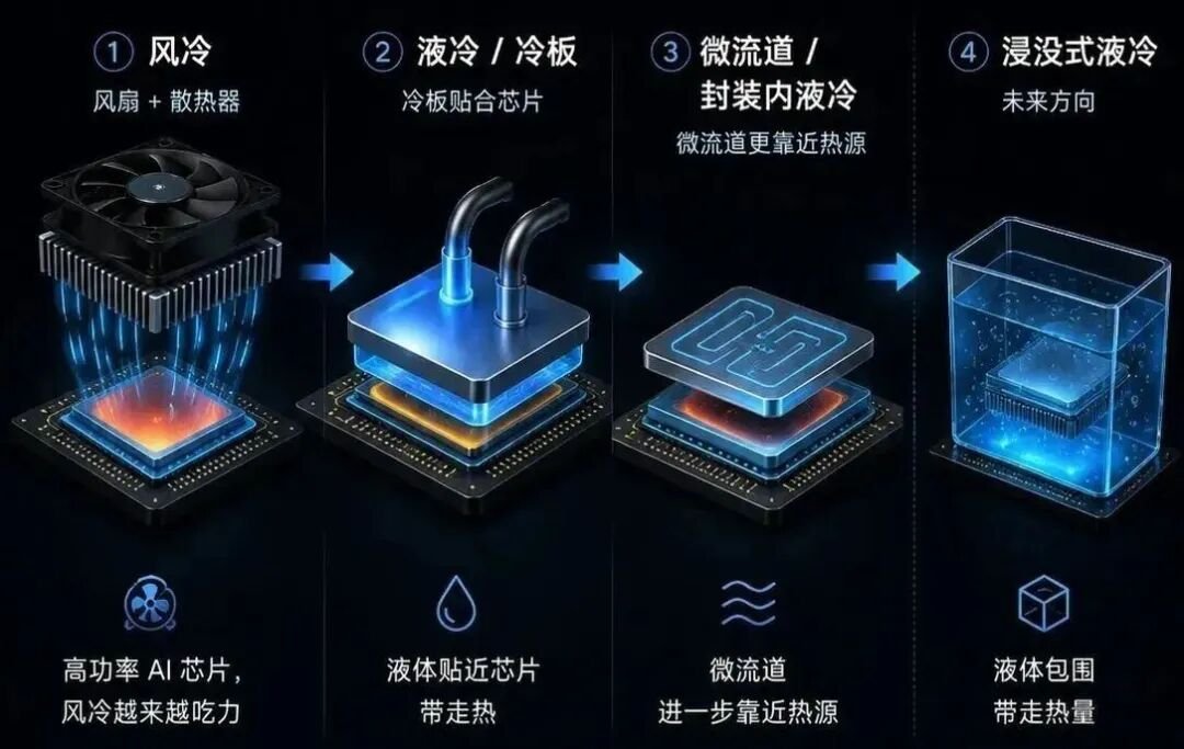
Cooling is transitioning from air to liquid. Air cooling: fans plus heatsinks. Liquid cooling/cold plates: cold plates attached to chips. Microchannel/immersion cooling: liquid flows close to or surrounds the chip.
The future direction is bringing liquid into regions closer to the package and silicon—the closer the coolant gets to the heat source, the higher the cooling efficiency.
7. Optimizing Power Delivery: Reducing I²R Losses
Traditional power delivery paths are long, resistive, and suffer high I²R losses—the power delivery network itself generates heat. Optimizing power paths—placing power closer to the chip, shortening current paths, lowering resistive losses—reduces heat generation. Backside power delivery, embedded capacitors, and decoupling capacitors all work to shorten current loops.
The goal isn’t to fight fires after heat appears, but to reduce wasteful heat generation at the source.
8. Thermal Simulation from Day One: Treating Heat as a Design Constraint
Thermal simulation analyzes temperature distribution, thermal resistance networks, hot spot prediction, and thermal bottleneck identification. Power integrity simulation examines IR drop, voltage droop, and power noise. Signal integrity analysis covers reflection, crosstalk, timing, and eye diagrams. Mechanical stress simulation evaluates thermal stress and deformation. System-level cooling simulation models airflow, liquid cooling, flow fields, and heat transfer.
The key isn’t post-hoc remediation but co-designing layout, structure, materials, and cooling upfront. Discovering overheating after the chip is fabricated makes changes prohibitively expensive.
Complete Thermal Chain at a Glance
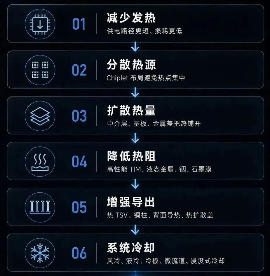
Advanced packaging thermal management is a multi-layered strategy: spreading heat sources through chiplet design, conducting heat laterally through interposers, optimizing TIM for efficient transfer, using IHS for heat spreading, creating vertical escape routes in 3D stacks, bringing coolant closer, reducing heat generation at the power delivery level, and simulating thermal behavior from the first design day. For high-performance AI chips, selecting the right monocrystalline silicon wafers and ensuring quality prime silicon wafers also plays a foundational role in overall thermal and mechanical performance.
Source: Original WeChat article