0.4–5μm L/SRDL Design Rules
1–8 LayersRDL Stack Height
10–500μmBump Pitch Range
200mm, 300mmWafer Diameters

Overview

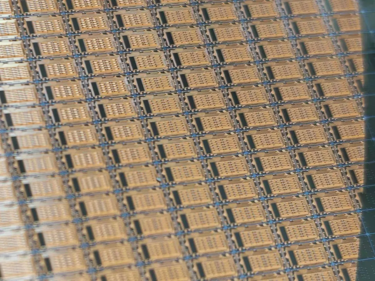
An RDL Bump Wafer is a fully processed wafer that has undergone redistribution layer (RDL) routing and bump interconnect formation — transforming standard IC bond pads into an optimized array of solder bumps, Cu pillars, or micro-bumps ready for flip-chip assembly or advanced packaging integration. This is the critical wafer-level interface between semiconductor fabrication and system-level packaging.

GINECHIP provides a complete RDL bump wafer service encompassing the entire process chain: UBM deposition, multi-layer RDL routing (standard 5μm to ultra-fine 0.4μm L/S), bump formation (solder, Cu pillar, micro-bump, Au stud), and final test/inspection. Wafers are delivered in standard cassettes, fully inspected, with comprehensive metrology and test data — ready for dicing and assembly at your OSAT partner or in-house packaging line.

RDL Technology Tiers

Standard RDL (5/5μm L/S)

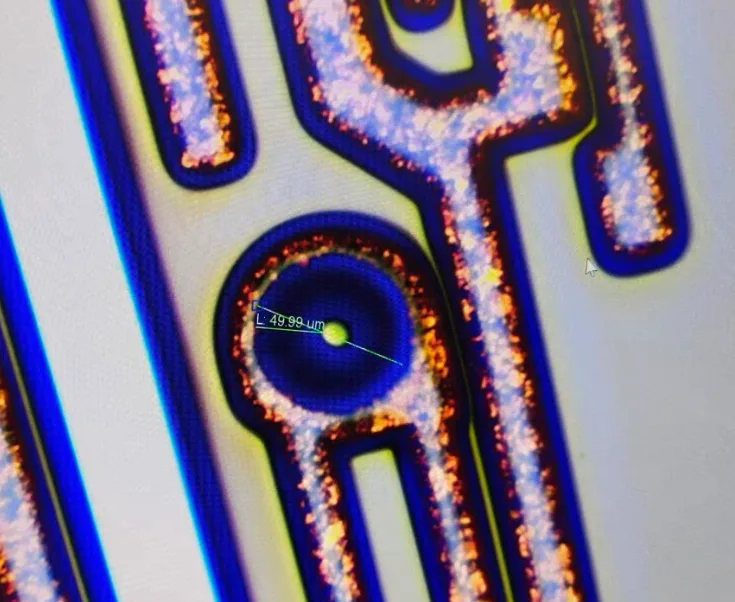
Single or dual-layer Cu redistribution routing with 5μm line/space design rules. Spin-coated polyimide (PI) dielectric with 20–30μm via openings. Suitable for fan-out wafer-level packaging (FOWLP), WLCSP pad relocation, and multi-chip module interconnects.

L/S: 5/5μmCu thickness: 5–8μmVia: 20–30μm diaPI dielectric: 5–8μm thickLayers: 1–3Bump pitch: 300–500μm

Fine-Line RDL (2/2μm L/S)

Advanced RDL with 2μm line/space capability using semi-additive plating (SAP) or Cu damascene processes. Low-k dielectric (BCB or advanced PI, k ≈ 2.6–3.0) for reduced inter-line capacitance. Enables higher routing density for high-I/O-count devices and multi-die fan-out packages.

L/S: 2/2μmCu thickness: 3–5μmVia: 10–15μm diaBCB or advanced PI dielectricLayers: 2–5Bump pitch: 130–300μm

Ultra-Fine RDL (0.4/0.4μm L/S)

Silicon interposer-grade RDL using Cu damascene process with SiO₂ dielectric. Sub-micron line/space for high-bandwidth die-to-die interconnects in 2.5D silicon interposer and high-density fan-out applications. CMP planarization after each metal layer for lithography depth-of-focus compatibility.

L/S: 0.4/0.4μmCu thickness: 1–3μmVia: 5–10μm diaSiO₂ dielectric (CVD)Layers: 2–8Damascene Cu + TaN/Ta barrier

Bump Interconnect Options

RDL routing is designed to terminate at bump pads — the physical interconnect between the IC and its packaging substrate. The table below summarizes our available bump technologies, which can be combined with any RDL tier.

Solder Bumps (C4)

Reflowable solder spheres on RDL pads for flip-chip attachment to organic substrates or ceramic packages. SAC305 (Sn96.5Ag3.0Cu0.5) is the standard Pb-free alloy. SnPb available for military/aerospace where RoHS exemption applies.

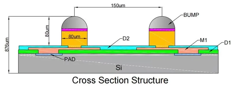
Alloys: SAC305, SAC405, SnPbPitch: 130–400μmHeight: 50–100μmUBM: Ti/Cu or TiW/CuReflow: wafer-level

Cu Pillar Bumps

Electroplated copper columns with SnAg solder cap. Superior electromigration resistance, finer pitch, and better thermal conductivity than solder bumps. Preferred for advanced nodes (sub-28nm) and high-density interconnects.

Pillar height: 20–80μmSolder cap: 10–25μm SnAgPitch: 40–130μmNi barrier optionAR: 2:1–5:1

Micro-Bumps (μ-Bump)

Ultra-fine-pitch Cu/Ni/SnAg bumps for die-to-die and die-to-wafer 3D stacking. Pitch as low as 10μm enables TB/s-class die-to-die bandwidth for HBM and chiplet architectures.

Pitch: 10–55μmDiameter: 5–25μmCu/Ni/SnAg stackHybrid bonding compatibleMass reflow or TCB

Complete Process Flow

01

Wafer Prep

Incoming wafer inspection. Passivation layer deposition (SiO₂ or SiN) if needed. Pad surface activation and cleaning for UBM adhesion.

02

UBM Deposition

PVD sputtering of UBM stack (Ti/Cu, TiW/Cu, etc.). Thickness uniformity < 3% (1σ). Adhesion and barrier layer optimization per bump alloy.

03

RDL Dielectric

Spin-coat and cure polyimide (PI) or BCB. Photo-definable or non-photo with dry etch via patterning. Via openings to UBM pads.

04

RDL Metal

Cu seed layer deposition (PVD). Photoresist patterning for RDL traces. Cu electroplating (SAP) or Cu damascene. Seed layer etch. CMP if damascene flow.

05

Multi-Layer Repeat

Dielectric + metal sequence repeated for each additional RDL layer. Via chain continuity tested at each layer for yield monitoring.

06

Passivation

Final passivation dielectric layer opening only at bump pad locations. Polyimide or SiN passivation. O₂ plasma descum before bump processing.

07

Bump Formation

UBM deposition on RDL pads. Thick photoresist patterning for bump definition. Electroplating (solder, Cu pillar) or stud bonding (Au). Resist strip + UBM etch.

08

Reflow &amp; Test

Solder reflow in N₂ or forming gas atmosphere. AOI for bump defects. Bump height coplanarity measurement. Electrical test (continuity, leakage). Singulation ready.

Key Applications

WLCSP (Wafer-Level CSP)

Single-die RDL redistribution from perimeter bond pads to area-array solder ball layout. Eliminates substrate, reduces package footprint to die size, and achieves < 0.5mm package height.

Fan-Out WLP (FOWLP)

RDL routing beyond die edges on molded reconstituted wafers. Enables higher I/O count than WLCSP while maintaining thin profile. Dominant packaging for smartphone PMICs and audio codecs.

2.5D Silicon Interposer

Passive Si interposer with multi-layer fine RDL and TSVs for GPU/CPU + HBM integration. Cu damascene RDL with 0.4/0.4μm L/S for > 10,000 die-to-die connections.

High-Density Fan-Out (HDFO)

Multi-die fan-out with fine-line RDL enabling inter-chip routing without silicon interposer. Lower cost alternative to 2.5D for mid-range I/O density applications.

RF/mmWave Front-End Module

Integrated passive devices (IPDs) on RDL layers — inductors, MIM capacitors, transmission lines — for impedance matching and filtering in compact RF front-end modules.

MEMS / Sensor WLP

RDL routing for MEMS sensor ASIC + MEMS die integration in wafer-level package. Through-silicon or through-mold vias for vertical interconnect in stacked sensor packages.

Integrated Passive Devices (IPD) on RDL

Beyond simple routing, RDL layers can implement high-quality passive components directly on the wafer — eliminating discrete SMD components and reducing module footprint. Our IPD-on-RDL capability includes: spiral inductors (Q > 30 at 2GHz, L = 0.5–20nH), MIM capacitors (Si₃N₄ or Al₂O₃ dielectric, 0.5–5pF, ±5% tolerance), thin-film resistors (NiCr or TaN, 10–1000 Ω/sq, ±10%), and transmission lines (CPW, microstrip for mmWave matching networks). IPD integration is particularly valuable for RF front-end modules where impedance matching network size and tolerance directly impact module performance.

Quality & Yield

RDL bump wafer processing includes multiple inspection and test gates: post-RDL electrical test (via chain continuity, isolation leakage), post-bump AOI (100% inspection for bump defects, bridging, missing bumps), bump height coplanarity (laser profilometry, ±2μm target for solder bumps, ±1μm for Cu pillars), shear strength testing (per JESD22-B117, statistical sampling), and X-ray inspection (void detection in Cu pillars and TSVs). Full lot traceability and Certificate of Conformance included.

Need RDL Bump Wafers for Your Design?

Provide your GDSII layout, pad list, RDL design rules, bump requirements, and wafer quantity — our advanced packaging team will deliver a comprehensive quotation within 24 hours.

ISO 9001:2015 GDSII Support AOI + Test JEDEC Qualified