60–80%Cost Savings vs Prime
Si · SiO₂ · Glass · Al₂O₃Material Options
Die to 300mm WaferFormat Range
Custom GeometriesFabrication Available

Overview

In any semiconductor fab or packaging facility, non-functional (dummy) wafers and dies are consumed daily for equipment qualification, process development, thermal profiling, and assembly line setup. Using production-grade prime wafers for these tasks is economically wasteful — a single 300mm prime wafer can cost $200–$500, while an equivalent dummy wafer costs a fraction of that.

GINECHIP provides a comprehensive range of dummy substrates engineered for these non-production applications: bare silicon dummy wafers in all standard diameters, oxidized dummy wafers for thermal process monitoring, singulated dummy dies for packaging R&D, patterned dummy dies with metal pad layouts for wire bonding and flip-chip development, glass and ceramic dummy substrates for specialized testing, and custom-fabricated dummy structures built to your specific test requirements.

Product Range

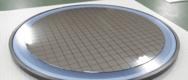
Dummy Silicon Wafers

Non-critical specification silicon wafers for mechanical testing, cassette filling, thermal uniformity verification, and equipment setup. Available in all standard diameters (100mm–300mm) with relaxed resistivity, type, and thickness specifications — providing significant cost savings versus prime or test-grade wafers.

Diameters: 100mm–300mmP-type or N-type (loose spec)Thickness: 200μm–1000μmAs-cut, lapped, or etched surfaceCassette quantity availableCost: 60–80% less than prime

Oxidized Dummy Wafers

Dummy wafers with a thermal SiO₂ coating (typically 100nm–2μm) for furnace tube fill, thermal process monitoring, and wafer handling system qualification. The oxide layer more closely mimics production wafer thermal mass and emissivity, improving process chamber thermal uniformity during qualification runs.

Oxide: 100nm–2μm thermal SiO₂Diameters: 100mm–300mmDry or wet oxidationUniformity: < 5% (relaxed spec)Backside: etched or polishedMulti-cycle usable

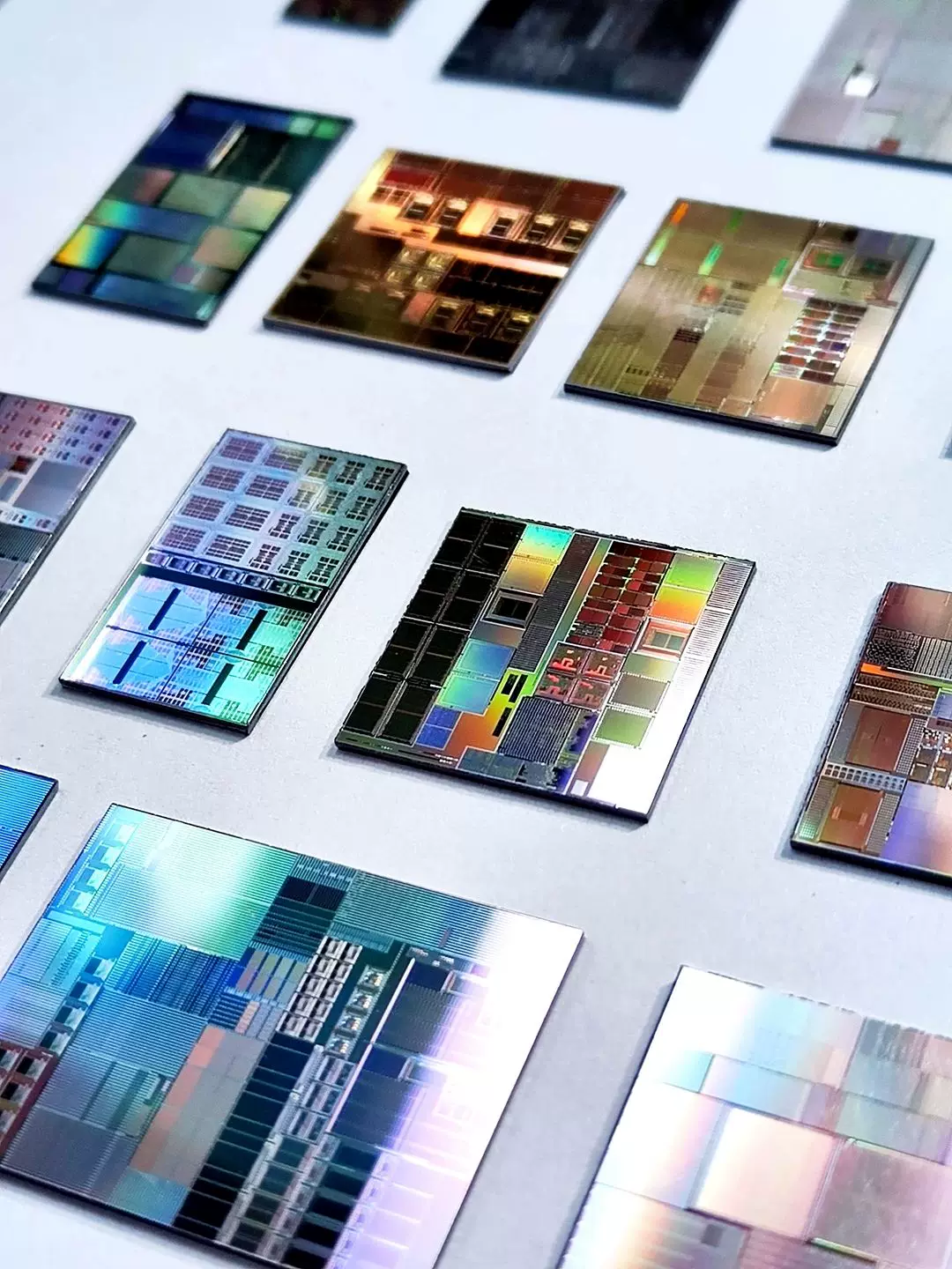
Dummy Dies — Silicon Chips

Singulated silicon die from non-critical wafers for package assembly process development, wire bonding parameter optimization, die-attach material evaluation, and flip-chip alignment calibration. Standard die sizes from 2mm × 2mm to 25mm × 25mm with various thickness options.

Die sizes: 2×2mm to 25×25mmThickness: 100μm–725μmSingulation: blade or stealth dicingBackside: lapped or polishedQuantity: 100–10,000+Custom sizes available

Dummy Dies — Patterned

Silicon dies with photolithographically defined metal patterns (Al or Au pads) mimicking production IC bond pad layouts. Enables realistic wire bonding and flip-chip process development without the cost of actual ICs. Custom pad layouts supported — provide your GDSII file.

Metal: Al (1μm) or Ti/AuPad pitch: 50–300μmPad opening: 40–150μmDie size: customPassivation: optional SiN or SiO₂GDSII layout accepted

Glass &amp; Ceramic Dummy Substrates

Non-silicon dummy substrates for packaging process development, laser dicing qualification, and thermal expansion mismatch studies. Glass (borosilicate, soda-lime), alumina (Al₂O₃), and aluminum nitride (AlN) substrates in wafer and coupon formats.

Glass: borosilicate, soda-limeCeramic: Al₂O₃ (96%, 99.6%)AlN: 170–230 W/m·KThickness: 200μm–1mmFormat: wafer or couponMetal coating optional

Custom Dummy Structures

Bespoke dummy wafers and dies fabricated to your specific requirements: through-wafer holes for gas flow testing, stepped-thickness wafers for height calibration, metal-coated strips for temperature sensor calibration, and wafer fragments for SEM sample mounting.

Custom geometries availableThrough-holes, slots, notchesMulti-thickness wafersMetal patterns (alignment marks)Fragment sizes: 5×5mm to 50×50mmDrawing-based fabrication

Common Applications

Equipment Qualification

Dummy wafers for new tool installation verification, preventive maintenance requalification, and chamber matching across multi-chamber cluster tools. Particle count and film thickness uniformity baselining.

Process Development

Patterned dummy dies for wire bonding recipe optimization, die-attach process window characterization, and flip-chip alignment calibration — without consuming expensive functional ICs.

Thermal Uniformity Mapping

Oxidized dummy wafers with thermocouple instrument holes for furnace tube profiling, RTP chamber temperature mapping, and hot-plate uniformity verification.

Package Assembly R&amp;D

Dummy dies in various sizes and thicknesses for package design validation, mold flow simulation, and assembly line qualification for new package formats (QFN, BGA, WLCSP).

University &amp; R&amp;D Labs

Cost-effective dummy substrates for student training on wafer handling, lithography alignment practice, and basic process familiarization — without the cost of device-grade wafers.

Cassette &amp; Automation Testing

Dummy wafers to fill cassette slots during partial-load processing, test wafer handling robot end-effectors, and validate SMIF/FOUP automation sequences.

Cost-Benefit Analysis

Prime vs Dummy Economics

A fabrication facility consuming 500 test/monitor wafers per month can reduce annual substrate spend by $1.5–3.0 million by substituting dummy wafers for non-critical applications. Dummy wafers cost 60–80% less than prime while providing functionally equivalent mechanical, thermal, and handling performance.

Total Cost of Ownership

Dummy wafers can often be reused across multiple qualification cycles — particularly for mechanical testing, cassette handling, and thermal profiling where the wafer surface quality is not critical. Combined with our wafer reclaim service, a single dummy wafer purchase can support dozens of qualification runs.

Patterned Dummy Die Design Support

For patterned dummy dies, we accept GDSII layout files defining your desired pad geometry and location. Our photolithography team will pattern a simple metal layer (Al or Ti/Au) on non-critical silicon wafers before dicing. Typical turnaround from layout to shipped dummy dies is 2–3 weeks. Ideal for companies developing new package formats who need realistic test vehicles for wire bonding, flip-chip, and die-attach process optimization.

Quality & Specifications

While dummy wafers and dies do not carry the same rigorous specifications as device-grade substrates, we maintain basic quality control: dimensional verification (thickness, diameter, die size), visual inspection (edge chips, cracks, surface contamination), cleanroom packaging (Class 1 compatible), and lot traceability. Oxidized dummy wafers include oxide thickness measurement data. Patterned dummy dies include pad dimension verification.

Need Dummy Substrates for Your Lab or Fab?

Specify the type, format, dimensions, and quantity you need — our team will provide availability and a cost-effective quotation within 24 hours.

ISO 9001:2015 Low Cost Bulk Discounts Custom Fabrication