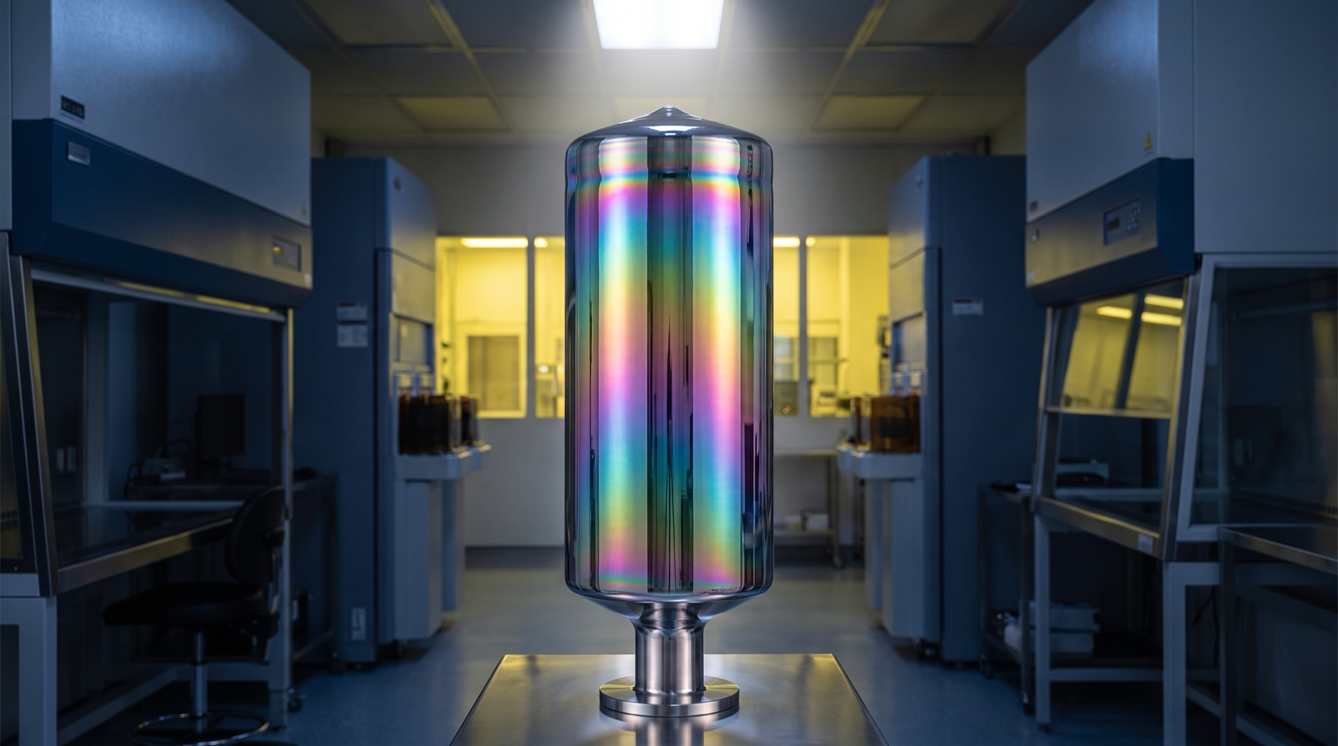
Silicon Ingots Bulk Sales
Bulk CZ/MCZ/FZ/Poly silicon ingots in diameters 100–450mm with 9N–11N purity (CZ/FZ) and 6N–7N (Poly). Available with CoA and SEMI-grade documentation.
Bulk Silicon Ingot Supply
GINECHIP supplies CZ, MCZ, FZ & polycrystalline silicon ingots. Available for diameters 100–450 mm and purity 9N–11N (N / P / intrinsic). Ingot length ranges from 200–2000 mm, with full CoA and conformity to SEMI standards.
Polycrystalline solar-grade silicon ingots (6N–7N) for cost-efficient photovoltaic production. Single-crystal silicon ingots support logic, memory, power and RF devices. N-type (P/As/Sb), P-type (B), and intrinsic FZ are available.
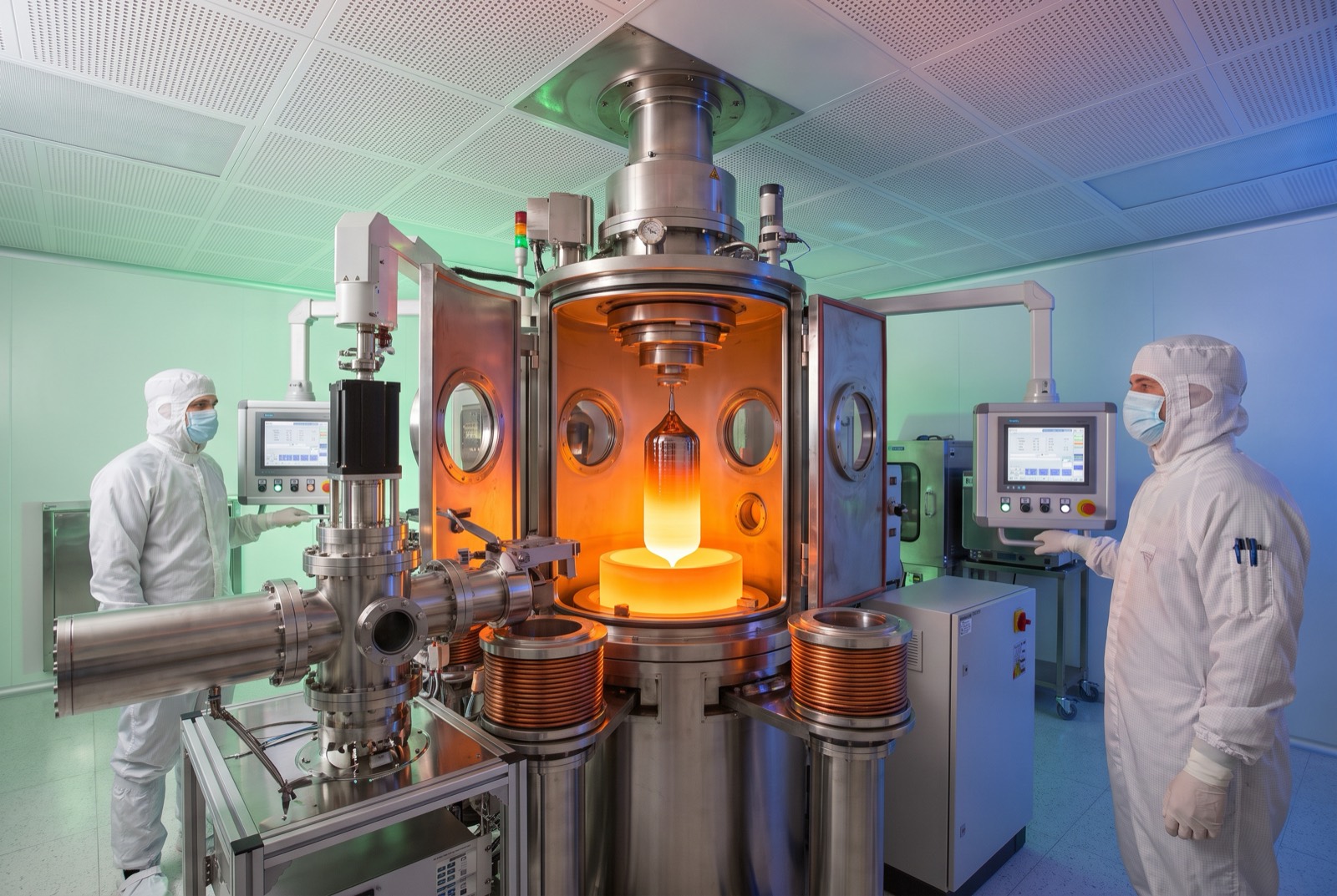
Growth Methods
We supply silicon ingots produced by four mainstream technologies: CZ, MCZ, FZ, and polycrystalline. Each route offers different trade-offs in cost, purity, and oxygen content.
CZ (Czochralski)
Most widely used growth method. CZ growth is a widely adopted method for producing silicon ingots with strong process maturity, reliable control of key crystal parameters and large-scale manufacturing. Choose CZ when you need proven yield and broad availability for wafer production.
- Diameter: 100mm – 450mm
- O₂ Content: 12 – 18 ppma
- Resistivity: 0.001 – 100 Ω·cm
- Cost: $ – $$
MCZ (Magnetic CZ)
Oxygen incorporation is tunable. MCZ delivers tighter oxygen management compared with conventional CZ. By using magnetic fields during growth, it helps tailor oxygen incorporation and support stable crystal quality. Ideal when you need controlled oxygen levels at scale.
- Diameter: 150mm – 300mm
- O₂ Content: 6 – 12 ppma
- Resistivity: 0.01 – 200 Ω·cm
- Cost: $$ – $$$
FZ (Float Zone)
No crucible-contact pollution. FZ growth produces silicon without the typical crucible contact, helping minimize container-related contamination. Choose FZ when ultra-low contamination and maximum electrical performance matter.
- Diameter: 100mm – 200mm
- O₂ Content: < 0.1 ppma
- Resistivity: 1 – 10,000+ Ω·cm
- Cost: $$$ – $$$$
Method Comparison
Choose the growth method based on your target device and manufacturing priorities: cost-focused selection with CZ, low-oxygen requirements with MCZ, and ultra-high purity needs with FZ.
CZ (Czochralski) — 100–450mm
Mature, widely adopted process with Oxygen content: 12–18 ppma and Resistivity: 0.001–100 Ω·cm. Ideal for high-volume production of logic and power devices.
- Best for: Logic / Memory / Power
- O₂: 12–18 ppma
MCZ Magnetic-Field Czochralski (150–300mm)
MCZ uses a magnetic field to suppress melt convection, enabling stable crystal growth and tighter oxygen content control for consistent bulk silicon ingots.
- High-throughput bulk production with controlled oxygen levels
- O₂: 6 – 12 ppma
FZ Float-Zone Silicon Ingots (100–200mm)
FZ (floating zone) grows silicon without a crucible, enabling the highest purity and excellent material quality for demanding processes.
- Ultra-high purity needs where maximum cleanliness is critical
- O₂: < 0.1 ppma
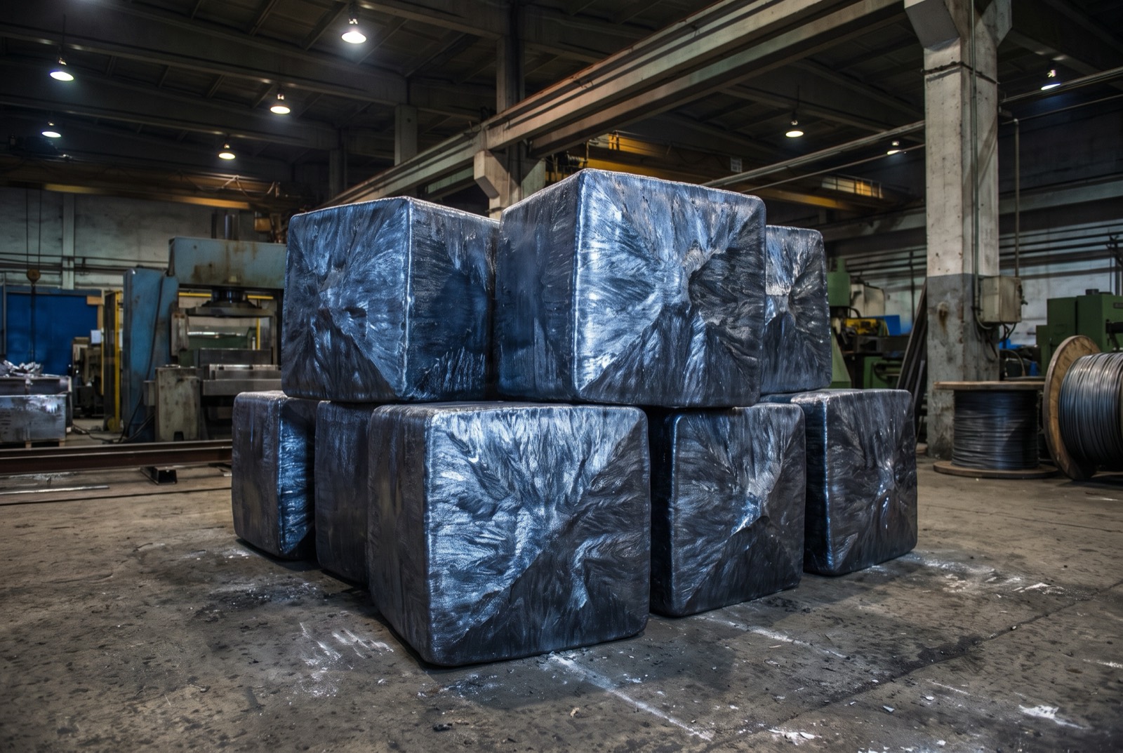
Multicrystalline Silicon Ingot
Batch supply of multicrystalline silicon ingots made by casting. Suitable for solar-grade applications and high-purity requirements with polycrystalline purity 6N–7N.
Featuring 156mm × 156mm square ingots, this product delivers strong cost performance for multicrystalline wafer production — ideal when you want cost advantage in planning.
Yield & Economics
Typical wafer yield estimates by ingot diameter, including saw kerf loss (180–200 μm, 160–180 μm, 140–160 μm depending on diameter).
| Ingot diameter | Wafer count per 10 cm | Wafer count per full ingot | Saw kerf loss |
|---|---|---|---|
| 150mm (6″) | ~66 | ~1,300 | 180 – 200 μm |
| 200mm (8″) | ~49 | ~1,000 | 180 – 200 μm |
| 300mm (12″) | ~33 | ~660 | 160 – 180 μm |
| 450mm (18″) | ~22 | ~440 | 140 – 160 μm |
Solar-grade vs Semiconductor-grade
Choose the right silicon ingot for your process — high-purity semiconductor-grade for ICs, or cost-effective solar-grade for PV.
Semiconductor-grade
9N–11N high-purity silicon ingots designed for IC applications, with low defects via Dash technology.
- Purity: 9N–11N
- No dislocations: Dash technique
Solar-grade mono-crystalline
CZ mono-crystalline solar silicon ingots for stable PV production and efficient cell manufacturing.
- Diameter: 100–450mm
- High-efficiency cells
Solar-grade poly-crystalline
Cast poly-crystalline solar silicon ingots — value focused for cost-effective PV manufacturing.
- Purity: 6N–7N
- Bar: 156mm×156mm
Quality & Certifications
Bulk sales with traceable documentation — ISO 9001:2015, aligned with SEMI standards, and delivered with CoA for each ingot.
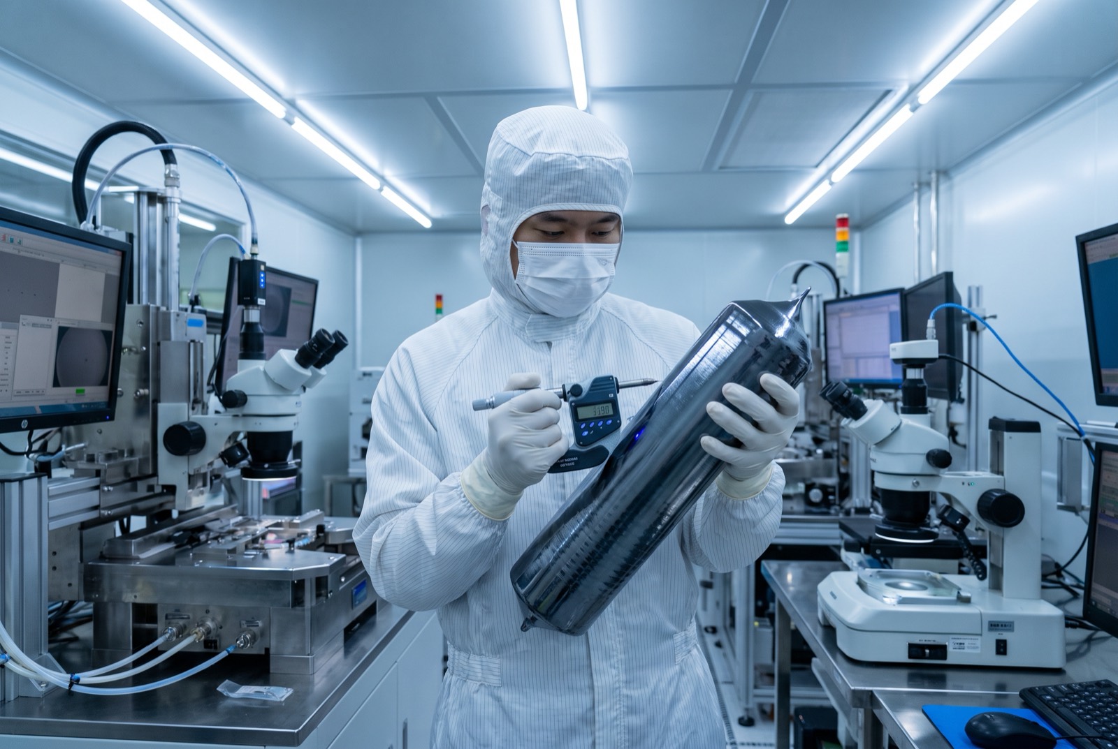
Technical Specifications
| Parameter | Specification |
|---|---|
| Growth Method | CZ (Czochralski), MCZ (Magnetic CZ), FZ (Float Zone), Multicrystalline (cast) |
| Diameter | 100mm, 125mm, 150mm, 200mm, 300mm, 450mm |
| Length | 200mm – 2000mm, custom lengths available |
| Dopant / Type | N-type (P, As, Sb), P-type (B), Intrinsic (FZ) |
| Resistivity | 0.001 – 10,000+ Ω·cm, application-dependent |
| Crystal Orientation | 〈100〉, 〈111〉, 〈110〉, off-cut available |
| Purity | 9N – 11N (CZ/FZ), 6N – 7N (multicrystalline) |
| Oxygen Content | CZ: 12 – 18 ppma, MCZ: 6 – 12 ppma, FZ: < 0.1 ppma |
| Carbon Content | CZ: ≤ 0.1 ppma, FZ: < 0.05 ppma |
| Lifetime | FZ: > 1,000 μs minority carrier lifetime |
| Dislocation Density | CZ: dislocation-free (Dash technique), Multi: 10³ – 10⁶/cm² |
| Ingot Shape | Cylindrical, square (156mm × 156mm for solar), rectangular |
| Edge Rounding | Ground, etched, as-cut |
| Surface Finish | As-grown, ground, etched, polished crown |
| Packaging | Wooden crate, foam-lined, vacuum-sealed, shock-resistant |
Application Areas
AI Chips
High-purity CZ/FZ silicon ingots for stable wafer production and reliable performance in AI and neural network accelerators, across 0.001 to 10,000+ Ω·cm.
Power Devices
Silicon ingots for power semiconductor manufacturing, supporting power management and power electronics. CZ/FZ 9N–11N and poly 6N–7N purity.
Solar PV
156mm×156mm solar-grade silicon ingots for photovoltaic cell production, with 0.001–10,000+ Ω·cm design flexibility.
MEMS
Silicon ingots for MEMS sensor and actuator fabrication, enabling consistent wafer quality for micromachined devices.
RF/Analog
High-purity silicon ingots support RF and analog wafers with stable electrical performance across a wide resistivity range.
Comms Equipment
Silicon ingots for communication devices enable reliable wafer fabrication for 5G and general transceiver applications.
Scientific Instruments
For detector and precision measurement wafers, high-purity silicon provides a strong foundation for performance and repeatability.
LED & Optoelectronics
Silicon ingots support consistent wafer processing for light-emitting and photodetector applications.
Bulk Pricing
High volume = better value. Quantity-based pricing is negotiable with a short lead time.
Polysilicon Ingot (Multi-Crystalline)
Solar-grade material with the lowest unit price, optimized for cost efficiency.
- Purity: 6N–7N
- Size: 156mm × 156mm square ingot
CZ Silicon Ingot
Suitable for both IC and solar applications — balanced performance and cost-effectiveness.
- Diameter: 100–450mm
- O₂: 12–18 ppma · Cost: $–$$
FZ Silicon Ingot
Highest purity choice for high-end applications, designed for demanding manufacturing.
- Purity: 9N–11N · O₂: <0.1 ppma
- Cost: $$$–$$$$
Supply Chain & Lead Time
Stable Supply
Stable supply backed by capacity planning for bulk silicon ingot needs — designed to support continuous production schedules.
Protected Logistics
Careful logistics and protection: wood crate, foam, vacuum sealing, and anti-vibration handling to safeguard material integrity.
Transparent Lead Time
Transparent lead time support with inventory coordination, helping you plan procurement with confidence for production continuity.
Custom Specifications
Need custom dimensions or specific specs? We'll help match your requirements and coordinate the right supply plan.
Bulk demand? Request a quote
Tell us your quantity, destination, and packaging preference — we'll respond with lead-time and pricing options for silicon ingot bulk orders.