
Advanced Compound Semiconductor Substrates – SiC, GaAs, GaN & InP
Silicon Carbide (SiC) Wafers
Our silicon carbide SiC wafers are premium wide-bandgap substrates critical for high-power, high-frequency, and high-temperature electronics. Available in 4H and 6H polytypes, primarily n-type, these substrates exhibit exceptional thermal conductivity (~3.7–4.9 W/cm·K), high breakdown electric field (~3 MV/cm), and superior hardness, making them ideal for power MOSFETs, Schottky diodes, IGBTs, and RF devices in electric vehicles, renewable energy inverters, rail traction, and aerospace applications. Grown via Physical Vapor Transport (PVT), our SiC wafers feature low micropipe density (<1/cm²), reduced basal plane dislocations, and tight resistivity control for optimal device performance.
With diameters up to 200 mm (8 inch) and beyond in development, these substrates support scalable production while maintaining crystalline quality. Surface finishes include CMP-polished epi-ready surfaces with ultra-low particle counts and minimal subsurface damage, ensuring high epitaxial layer quality for subsequent SiC epitaxy. Full traceability, laser marking options, and certificates of analysis accompany every wafer, meeting automotive-grade (AEC-Q101) and industrial reliability standards.
As the transition to electrification and 5G/6G accelerates demand for efficient power conversion, our high-quality SiC wafers deliver the consistency and performance required to achieve higher switching frequencies, reduced losses, and compact system designs. Rigorous quality controls including X-ray diffraction, Raman spectroscopy, and KOH etching verification guarantee defect minimization.
Technical Data Specification
| Parameter | Specification |
|---|---|
| Polytype | 4H (dominant) / 6H |
| Dopant Type | N-type (Nitrogen) |
| Resistivity | 0.015–0.025 Ω·cm (typical) |
| Diameter | 100 mm / 150 mm / 200 mm |
| Thickness | 350 ± 25 µm (standard) |
| Micropipe Density | ≤ 1 / cm² |
| Dislocation Density | EPD ≤ 5000 / cm² |
| TTV | ≤ 5 µm |
| Bow / Warp | ≤ 40 µm |
| Surface Finish | CMP epi-ready both sides |
| Particles (@ ≥0.2 µm) | ≤ 50 / wafer |
| Thermal Conductivity | ≥ 370 W/m·K |
| Breakdown Field | ~3 MV/cm |
| Orientation | (0001) off-axis 4° ± 0.5° |
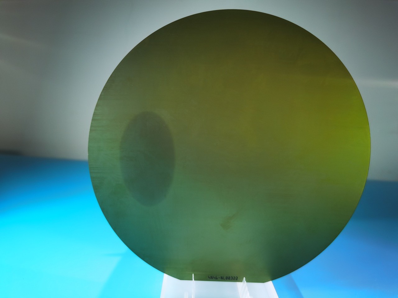
Gallium Arsenide (GaAs) Wafers
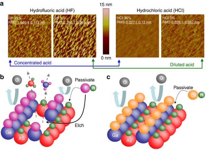
Gallium arsenide GaAs wafers are compound semiconductor substrates renowned for their high electron mobility (up to 8500 cm²/V·s), direct bandgap (1.42 eV), and excellent optoelectronic properties. These semi-insulating or doped wafers serve as the foundation for high-frequency RF devices (pHEMT, HBT), microwave/mmWave circuits, optoelectronics (LEDs, lasers, detectors), and high-efficiency solar cells. Grown via Vertical Gradient Freeze (VGF) or Liquid Encapsulated Czochralski (LEC), our GaAs substrates offer low dislocation density, uniform electrical characteristics, and superior surface quality for epitaxial growth of complex heterostructures.
Available in diameters 100–150 mm with semi-insulating (SI) resistivity >10⁷ Ω·cm or n/p-type doping, these wafers support advanced processes including MOCVD and MBE epitaxy. Tight control over carbon/oxygen impurities, etch pit density, and flatness ensures high-yield fabrication of GaAs-based devices for 5G infrastructure, satellite communications, defense radar, and photonics applications.
Our supply emphasizes cleanroom packaging, full traceability, and detailed characterization to meet stringent requirements of telecom, aerospace, and photonic industries. As demand for higher bandwidth and efficiency grows, GaAs substrates remain essential for performance-critical applications where silicon falls short.
Technical Data Specification
| Parameter | Specification |
|---|---|
| Diameter | 100 mm / 150 mm |
| Type | Semi-insulating / N-type / P-type |
| Resistivity (SI) | > 1×10⁷ Ω·cm |
| Dopant (doped) | Si / Zn / C (custom) |
| Carrier Concentration | 1×10¹⁶ – 1×10¹⁸ cm⁻³ |
| Dislocation Density (EPD) | ≤ 5000 / cm² |
| Thickness | 625 ± 25 µm |
| TTV | ≤ 3 µm |
| Bow / Warp | ≤ 10 µm |
| Surface Finish | Epi-ready CMP |
| Particles (@ ≥0.16 µm) | ≤ 20 / wafer |
| Electron Mobility | ≥ 6000 cm²/V·s |
| Orientation | (100) ± 0.5° |
| Packaging | Double-sided protection |
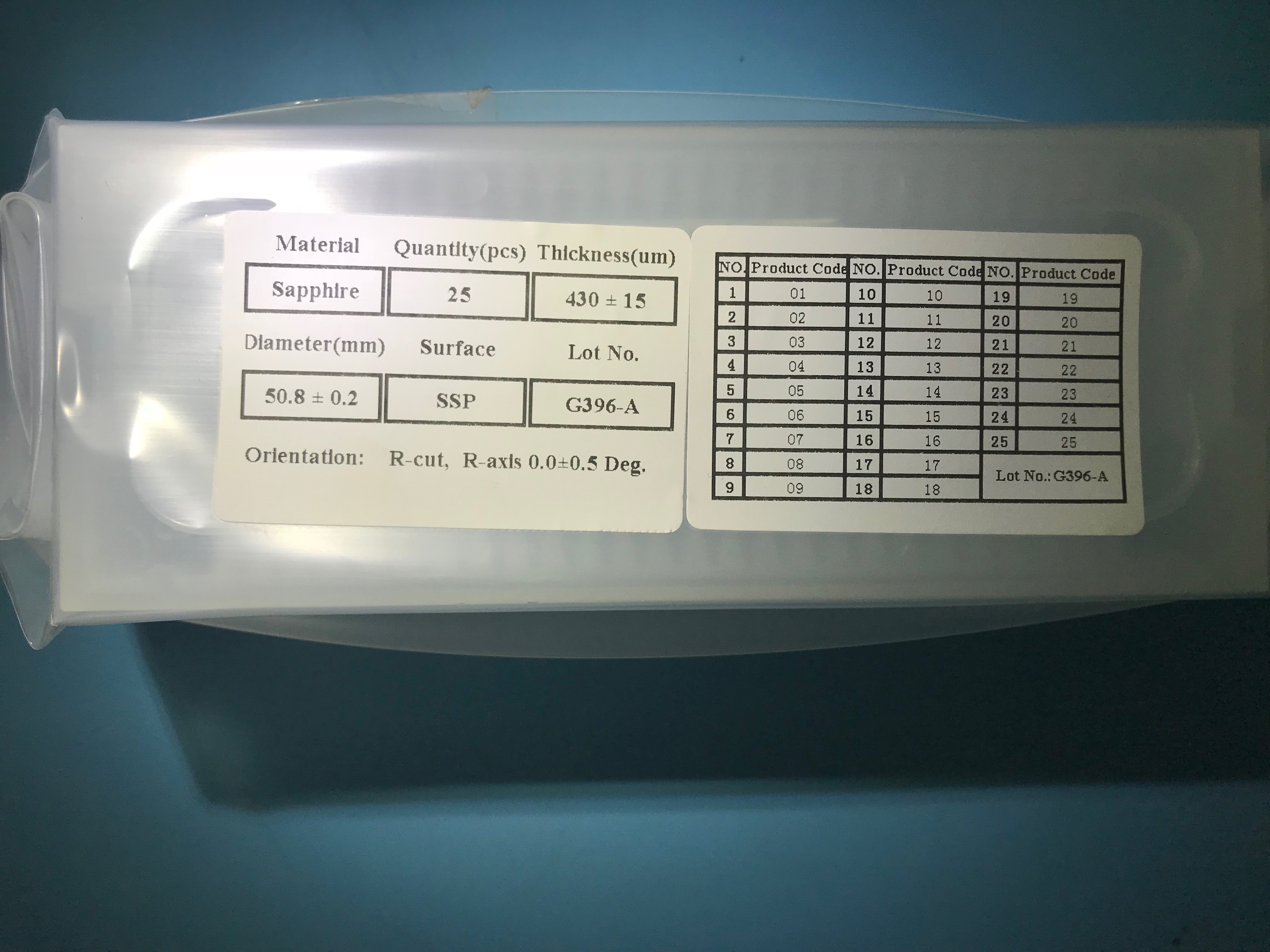
Gallium Nitride (GaN) on Sapphire
GaN on sapphire wafers combine the superior properties of gallium nitride (wide bandgap 3.4 eV, high breakdown field ~3.3 MV/cm, high saturation velocity) with cost-effective, large-diameter sapphire substrates. These templates are widely used for high-brightness LEDs, power HEMTs, RF amplifiers, and laser diodes. Grown via MOCVD, our GaN layers offer excellent uniformity, low defect density, and optimized strain management for high-performance devices in lighting, power electronics, and wireless communications.
Available in 2–6 inch formats with GaN thicknesses from 1–7 µm, often including AlGaN buffer layers for crack prevention and improved crystal quality. Sapphire's transparency and thermal stability make it ideal for optoelectronic applications, while GaN enables high-efficiency power switching and high-frequency operation beyond silicon limits.
Our products undergo rigorous metrology (XRD, AFM, PL mapping) to ensure low threading dislocation density and high wafer-to-wafer consistency, supporting volume production for automotive, consumer electronics, and 5G base stations. As the compound semiconductor market expands, GaN on sapphire remains a cornerstone for energy-efficient technologies.
Technical Data Specification
| Parameter | Specification |
|---|---|
| Substrate | Sapphire (c-plane) |
| Diameter | 50.8 mm / 100 mm / 150 mm |
| GaN Thickness | 1–7 µm (custom) |
| Buffer Layer | AlGaN / GaN multilayer |
| Dislocation Density | ≤ 5×10⁸ / cm² |
| Surface Roughness (RMS) | ≤ 0.5 nm |
| Wafer Bow | ≤ 30 µm |
| Uniformity (thickness) | ≤ ±5% |
| Carrier Concentration | Undoped or Si-doped |
| Orientation Off-cut | 0.2° ± 0.1° |
| Particles | ≤ 30 / wafer |
| Application | LED / Power / RF |
| Traceability | Lot-level CoC |
Indium Phosphide (InP) Wafers
Indium phosphide InP wafers are high-performance III-V substrates prized for their direct bandgap (1.35 eV), high electron mobility (>5000 cm²/V·s), and compatibility with long-wavelength optoelectronics. Used extensively in photonic integrated circuits, high-speed transceivers (100G–800G+), lasers, photodetectors, and THz devices, InP enables low-loss, high-speed optical communication for data centers, telecom networks, and sensing applications.
Grown via VGF or LEC methods, our substrates provide low etch pit density, uniform doping, and epi-ready surfaces optimized for MOCVD/InP-based epitaxy. Diameters range from 50–100 mm (scaling to 150 mm), with semi-insulating (Fe-doped) or n-type options. Advanced lattice-matched structures support complex heterostructures like InGaAsP/InP for DWDM systems and coherent optics.
With increasing bandwidth demands in AI-driven networks and 6G, our InP substrates deliver the reliability and performance needed for next-generation photonics. Strict quality assurance including Hall measurement, PL mapping, and defect scanning ensures consistency for high-yield manufacturing.
Technical Data Specification
| Parameter | Specification |
|---|---|
| Diameter | 50 mm / 76 mm / 100 mm |
| Type | Semi-insulating (Fe) / N-type (S) |
| Resistivity (SI) | > 1×10⁷ Ω·cm |
| Dopant Concentration | 1×10¹⁸ cm⁻³ (typical doped) |
| Dislocation Density (EPD) | ≤ 5000 / cm² |
| Thickness | 350 ± 25 µm |
| TTV | ≤ 3 µm |
| Bow / Warp | ≤ 15 µm |
| Surface Finish | Epi-ready CMP |
| Particles (@ ≥0.16 µm) | ≤ 20 / wafer |
| Electron Mobility | ≥ 4000 cm²/V·s |
| Orientation | (100) ± 0.5° |
| Packaging | Single/double protection |